
Iii-v depletion mode semiconductor device

a semiconductor device and depletion mode technology, applied in the field of semiconductor devices, can solve the problems of obstructing the path for carriers to flow from the source to the drain, obstructing the path for carriers to flow, and reducing the on-state resistance compared to silicon-based devices with the same breakdown voltage, etc., to facilitate the depletion of 2d carrier gas.

Active Publication Date: 2020-11-12
CAMBRIDGE GAN DEVICES LIMITED
View PDF0 Cites 7 Cited by
  • Summary
  • Abstract
  • Description
  • Claims
  • Application Information

AI Technical Summary

Benefits of technology

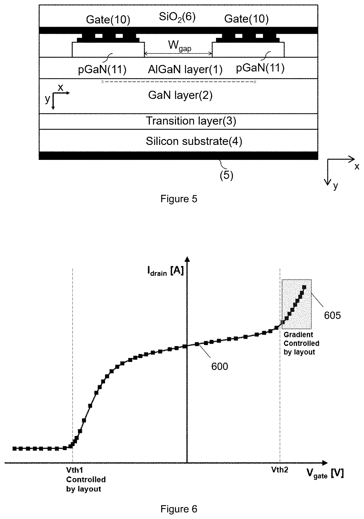
The proposed device allows for control of its threshold voltage through changes to its layout design, rather than only through adjustments to epitaxial growth or the gate metal stack. This results in an optimized device at a lower cost and effort. The active gate terminal can have either an Ohmic contact or a Schottky contact, with the latter being more stable but resulting in slightly higher gate leakage currents. The device is designed to passivate traps in the AlGaN and GaN buffers by hole injection.

Problems solved by technology

The wide band gap of the material (Eg=3.39 eV) results in high critical electric field (Ec=3.3MV / cm) which can lead to the design of devices with a shorter drift region, and therefore lower on-state resistance if compared to a silicon-based device with the same breakdown voltage.
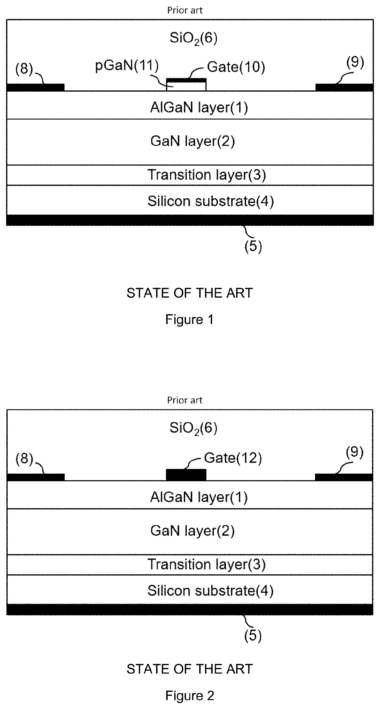
However, the 2DEG which inherently exists at the AlGaN / GaN hetero-interface creates a challenge when attempting the design of enhancement mode rather than depletion mode devices.
Therefore to adjust the threshold voltage to a level which is most suitable for a specific application would require a change in the epitaxial growth and / or the gate metal processing, which is time consuming and expensive.
When the gate voltage is very negative, the adjacent highly doped semiconductor islands deplete the portion of the 2D carrier gas between them, obstructing the path for carriers to flow from the source to drain.
This is characterised by a steep increase in current and, as a result, a steep decrease in the on-state resistance.
A certain amount of hole current through the gate has a positive effect on the stability of the device during dynamic high voltage stress, but if the current is too high this is seen as leakage in the control terminal affecting the driver and the total losses of the device.
The device according to this disclosure can be monolithically integrated with other high voltage or low voltage normally-off devices.

Method used


Image

  • Iii-v depletion mode semiconductor device
  • Iii-v depletion mode semiconductor device
  • Iii-v depletion mode semiconductor device

Examples


Embodiment Construction

[0077]The present disclosure will be understood more fully from the accompanying drawings, which however, should not be taken to limit the disclosure to the specific embodiments shown, but are for explanation and understanding only.

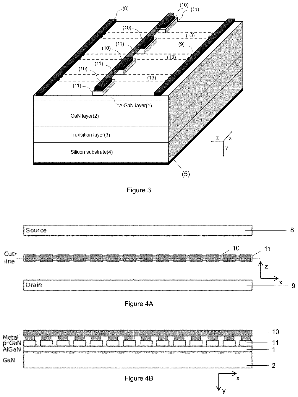
[0078]FIG. 3 shows a schematic perspective view of the active area of a GaN based semiconductor device according to an embodiment of the present disclosure. The device is presented in three dimensions: a first dimension (z-direction), a second dimension (x-direction) and a third dimension (y-direction).

[0079]In this embodiment, the device comprises a semiconductor (e.g. silicon) substrate 4 defining a major (horizontal) surface at the bottom of the device. It will be appreciated that any other substrates for GaN devices can be used. Examples of alternative substrate material are Sapphire, Silicon Carbide, and GaN.

[0080]Below the substrate 4 there is a substrate terminal 5. The device includes a transition layer 3 formed on top of the semiconductor substra...


PUM

PropertyMeasurementUnit
distanceaaaaaaaaaa
bias voltageaaaaaaaaaa

Abstract

We disclose herein a depletion mode III-nitride semiconductor based heterojunction device, comprising: a substrate; a III-nitride semiconductor region formed over the substrate, wherein the III-nitride semiconductor region comprises a heterojunction comprising at least one two-dimensional carrier gas of second conductivity type; a first terminal operatively connected to the III-nitride semiconductor region; a second terminal laterally spaced from the first terminal in a first dimension and operatively connected to the III-nitride semiconductor region; at least two highly doped semiconductor regions of a first conductivity type formed over the III-nitride semiconductor region, the at least two highly doped semiconductor regions being formed between the first terminal and the second terminal; and a gate terminal formed over the at least two highly doped semiconductor regions; wherein the at least two highly doped semiconductor regions are spaced from each other in a second dimension.

Description

FIELD OF THE DISCLOSURE[0001]The present disclosure relates to semiconductor devices. Particularly, but not exclusively, the disclosure relates to hetero-structure AlGaN / GaN high electron mobility transistors or rectifiers.BACKGROUND OF THE DISCLOSURE[0002]Gallium Nitride (GaN) is a wide band gap material with properties that make it a suitable candidate for use in several fields of application (e.g. radio-frequency electronics, opto-electronics, power electronics) which require solid-state devices.[0003]GaN technology allows transistors with high electron mobility and high saturation velocity to be designed. These properties of GaN have made it a good candidate for high-power and high-temperature microwave applications, for example radar and cellular communications systems. As systems expand in subscribers and desired capacity, interest in increasing their operating frequency and power has grown correspondingly. Higher frequency signals can carry more information (bandwidth) and al...

Claims


Application Information

Patent Timeline
Patent Type & Authority Applications(United States)
IPC IPC(8): H01L29/778H01L29/20H01L29/205H01L29/66H01L21/02H01L27/07
CPCH01L29/2003H01L29/66462H01L29/7786H01L21/0254H01L27/0727H01L29/205H01L21/8252H01L27/0605H01L27/085H01L27/0883H01L29/1066H01L29/861
Inventor UDREA, FLORINEFTHYMIOU, LOIZOSLONGOBARDI, GIORGIAARNOLD, MARTIN
Owner CAMBRIDGE GAN DEVICES LIMITED
Learn More