
Transition-metal oxides-coated hydrogen-terminated diamond surface and uses thereof

a hydrogen-terminated diamond surface and transition metal oxide technology, applied in non-metal conductors, electric discharge tubes, semiconductor devices, etc., can solve the problems of loss of conductivity upon heating, no satisfactory and robust solution has yet been offered for ensuring sustainability, and all the above approaches have considerable limitations

Active Publication Date: 2020-12-24
TECHNION RES & DEV FOUND LTD
View PDF0 Cites 2 Cited by
  • Summary
  • Abstract
  • Description
  • Claims
  • Application Information

AI Technical Summary

Benefits of technology

The present invention provides a conducting material made of a carbon-based material, such as diamond or insulating diamond-like carbon, with a layer of tungsten trioxide, rhenium trioxide, or chromium oxide coating its hydrogen-terminated surface. This material can be used in electronic components, sensors, and field emission electron sources. The technical effect is the improved electrical conductivity and stability of the carbon-based material, making it useful in a variety of applications.

Problems solved by technology

In light of this wide spectrum of promising applications, a lot of efforts are invested for recognizing new surface electron acceptors with ability to surpass existing fragile surface TD of diamond:H. Among all the exposed surface acceptor candidates studied so far, none have yet offered a satisfactory and robust solution for assuring sustainability and efficiency of the diamond surface conductivity as they are required for practical electronic device processing and reliability.
Nevertheless, all those proposed surface electron acceptor molecules were still suffering from instability to temperature fluctuations, resulting in loss of conductivity upon heating (Laikhtman et al., 2004).
However, despite the ameliorations, all the above approaches have considerable limitation such as in the design, process, and architecture of diamond:H-based electronic devices because the resulting 2DHG conductive channel must be protected with an additional impeding capsulation layer.

Method used


Image

  • Transition-metal oxides-coated hydrogen-terminated diamond surface and uses thereof
  • Transition-metal oxides-coated hydrogen-terminated diamond surface and uses thereof
  • Transition-metal oxides-coated hydrogen-terminated diamond surface and uses thereof

Examples


examples

[0050]Study 1. Boosting Surface Charge-Transfer Doping Efficiency and Robustness of Diamond with WO3 and ReO3

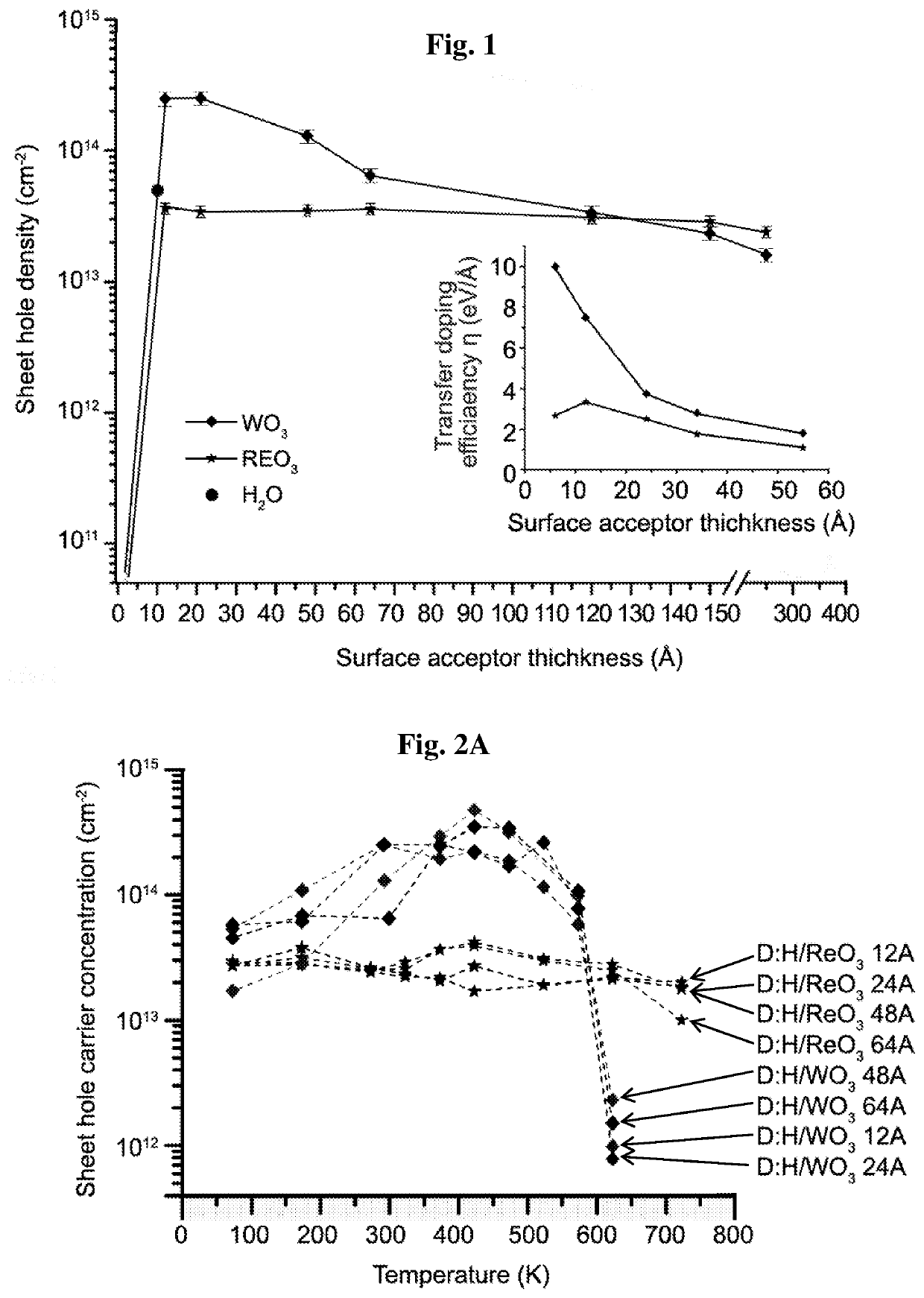
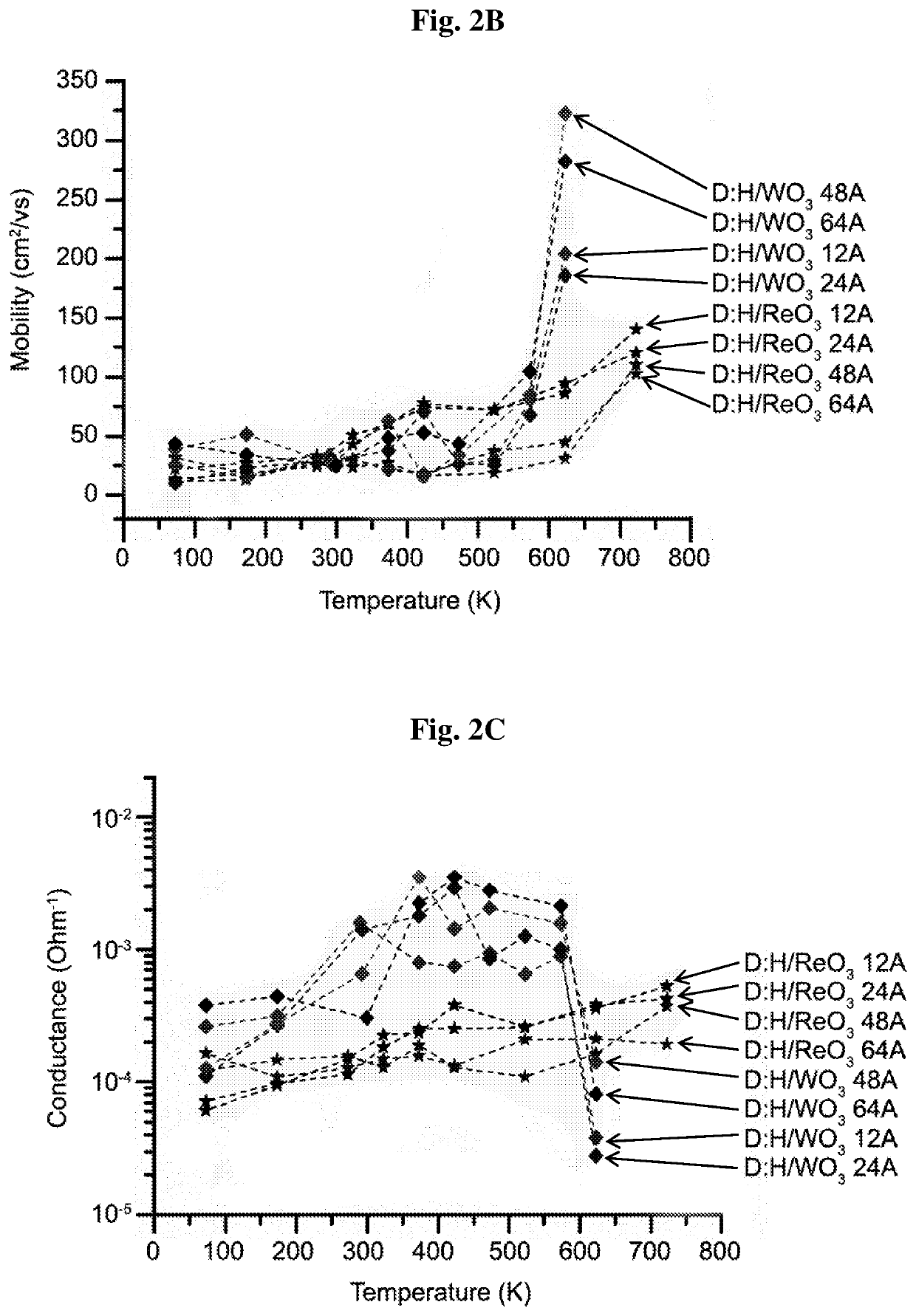
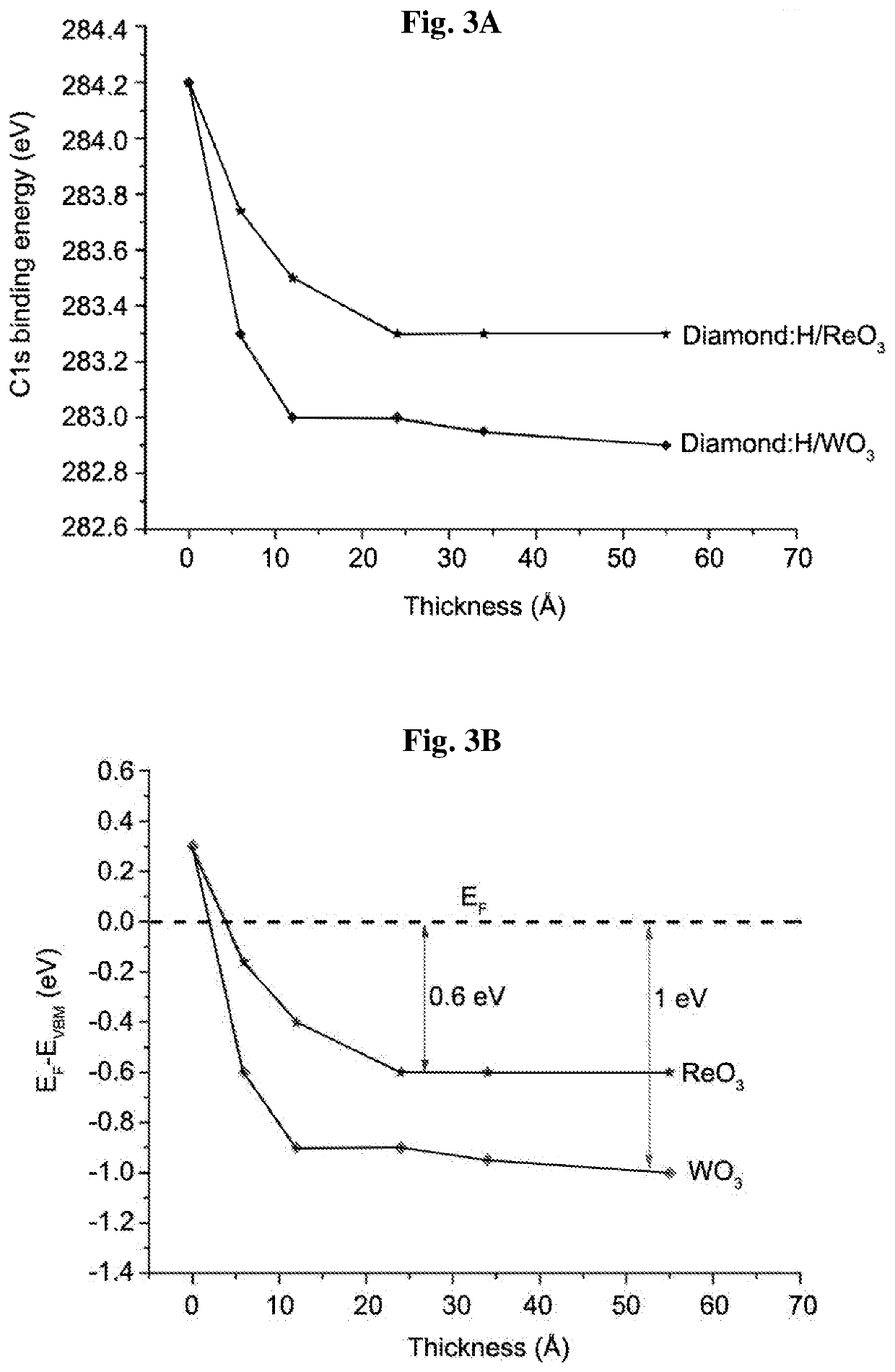
[0051]Disclosed herein is the use of WO3 and ReO3 as direct surface electron acceptor layers for the TD of the diamond:H surface. WO3 TD is found to yield a p-type conductive surface layer at a close diamond:H interface proximity with electrical properties significantly superior to those induced by other materials reported so far (FIG. 1). The areal hole density at room temperature vs. thickness coverage, as measured by Hall effects, is found to reach a record value of up to 2.52×1014 cm−2 at the very first monolayers of coverage (from 1.2 nm to 4.8 nm) for WO3. For ReO3, a value in the range of 2.87-3.63×1013 cm−2 is shown for the different thicknesses. Hall effect measurements as a function of temperature for diamond:H / ReO3 layers show an impressive electrical stability of up to at least 450° C., while diamond:H / WO3 loses its high electrical performance after 300° C.

[0052]...


PUM

PropertyMeasurementUnit
sheet conductanceaaaaaaaaaa
widthaaaaaaaaaa

Abstract

The present invention provides a conducting material comprising a carbon-based material selected from a diamond or an insulating diamond-like carbon, having a hydrogen-terminated surface and a layer of tungsten trioxide, rhenium trioxide, or chromium oxide coating said hydrogen-terminated surface. Such conducting materials are useful in the fabrication of electronic components, electrodes, sensors, diodes, field effect transistors, and field emission electron sources.

Description

TECHNICAL FIELD[0001]The present invention relates to a conductive diamond surface, more particularly to tungsten trioxide (WO3), rhenium trioxide (ReO3), or chromium oxide (CrO3)-coated hydrogen-terminated diamond surface showing thermal stability with superior sheet conductivity and hole carrier concentration, and to uses thereof.BACKGROUND ART[0002]The next-generation of outperforming electronic devices is predicted to be led by diamond implementation as extreme semiconductors, as they have the most favorable properties among other semiconductors for this task (i.e., highest breakdown field and thermal conductivity, dielectric constant, and carrier transport properties). Up to date, due to the lack of suitable bulk dopants (acceptors and donors) with low activation energies (Kalish, 2007), diamond free carriers are found only at the surface and are generated by an unique sub-surface two-dimensional hole gas (2DHG) (Strobel et al., 2004; Chakrapani et al., 2007). This 2DHG is form...

Claims


Application Information

Patent Timeline
Patent Type & Authority Applications(United States)
IPC IPC(8): H01L29/16H01B1/04H01B1/08H01J37/073H01L29/778H01L29/872H01L29/167
CPCH01B1/04H01L29/872H01L29/7786H01J37/073H01B1/08H01L29/167H01L29/1602H01L29/267C01B32/25
Inventor KALISH, RAFITORDJMAN, MOSHE
Owner TECHNION RES & DEV FOUND LTD
Learn More