Electrode structure, manufacturing method therefor, and electrochemical element comprising same
- Summary
- Abstract
- Description
- Claims
- Application Information
AI Technical Summary
Benefits of technology
Problems solved by technology
Method used
Image

Examples
example 1
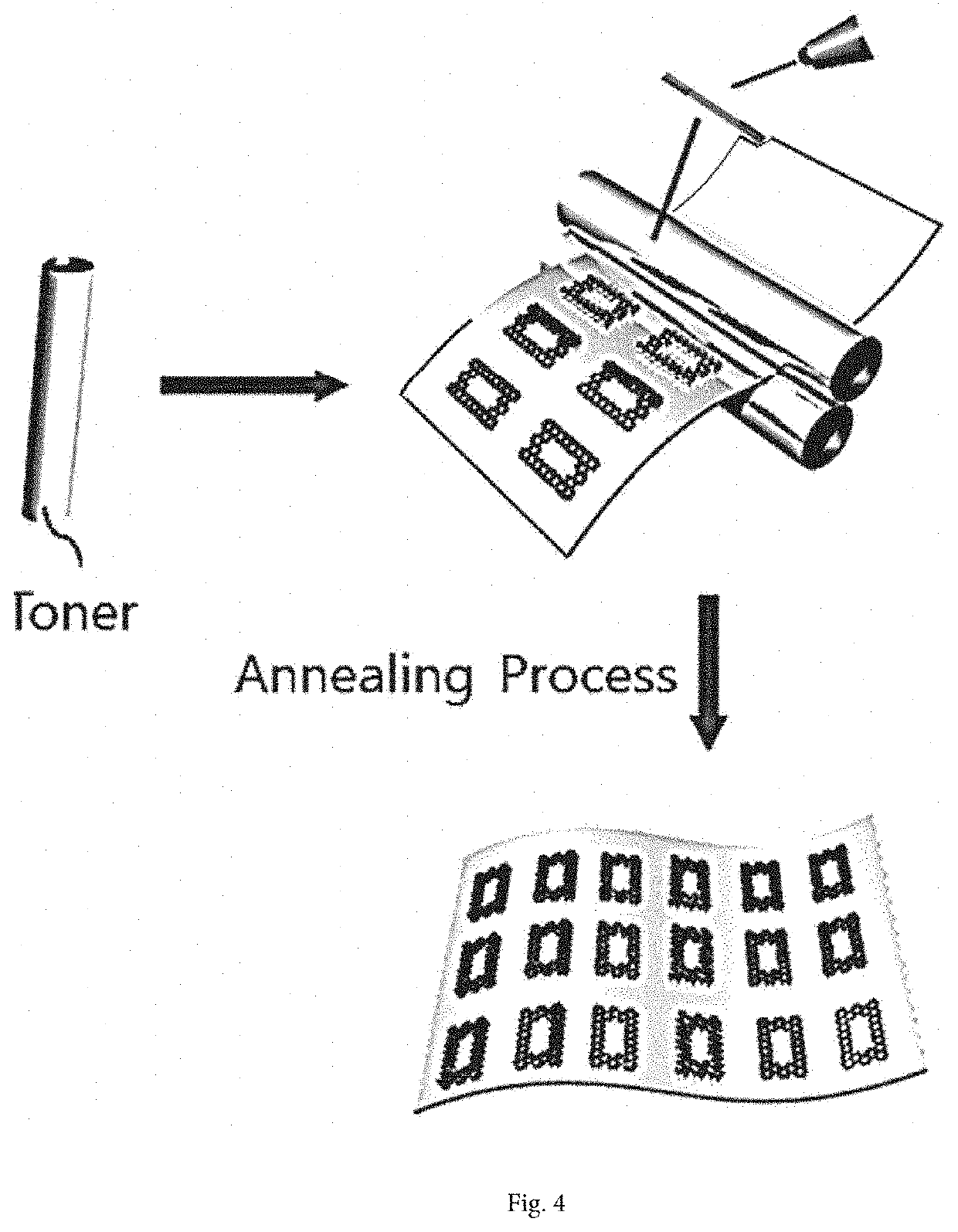
[0094]A copper foil (Alfa Aesar, 99.999%) was prepared, and a printed layer having an electrode pattern was formed directly on the copper foil by laser printing using Fuji Xerox CP405d and a laser printer toner cartridge thereof.
[0095]The copper foil having the printed layer formed thereon was provided in a chamber into which a gas mixture of hydrogen gas with a flow rate of 50 sccm and argon gas with a flow rate of 500 sccm was injected. The copper foil was heated in a furnace at a temperature of about 800° C. in the chamber for about 30 minutes. Furthermore, the copper foil having the printed layer formed thereon was taken out of the furnace and cooled at room temperature (25° C.) to form an electrode structure.
[0096]A field emission scanning electron microscope (FE-SEM; AURIGA Carl Zeiss) was used to observe the surface structure of the electrode structure fabricated in Example 1, and a transmission electron microscope (TEM; JEOL JEM-2100) was used to observe the morphology of th...
example 2
[0100]An electrode structure was fabricated in the same manner as in Example 1 above, except that a 99.9% pure nickel foil was used.
[0101]FIG. 9 shows an FE-SEM image of the electrode structure fabricated according to Example 2. Referring to FIG. 9, it can be confirmed that spherical graphitic carbon nanoparticles were formed on the surface of an electrode pattern in a region (Patterned) in which the electrode pattern was formed, unlike a region (Non-patterned) in which no electrode pattern was formed.
[0102]FIG. 10 shows a cross-sectional FE-SEM image of the electrode structure fabricated according to Example 2, and it can be seen that a graphene-graphitic carbon composite layer was formed on the nickel foil to have a thickness of about 13 μm. Since the carbon solubility of nickel at high temperature is higher than the carbon solubility of copper at high temperature, it can be seen that the thickness of the graphene-graphitic carbon composite layer formed on the nickel foil is large...
experimental example 4
[Experimental Example 4]—Adhesion Test
[0114]For an adhesion test for an electrode structure sample prepared in the same manner as in Example 1, a peel-off test was performed using a method of attaching a commercial tape (3M company) to the surface of the sample by pressing with hand, and then peeling-off the tape with hand.
[0115]FIG. 16 shows a peel-off test image according to Experimental Example 4. Referring to FIG. 16, as a result of performing the peel-off test, it can be confirmed that the graphene-graphitic carbon composite layer of the electrode structure did not leave a stain on the tape.
[0116]In addition, for the adhesion test, a rubbing test was performed using a method of rubbing the surface of the electrode structure sample, prepared in the same manner as in Example 1, with a rubber-gloved-hand.
[0117]FIG. 17 shows a rubbing test image according to Experimental Example 4. Referring to FIG. 17, as a result of performing the rubbing test, it can be confirmed that the graphe...
PUM
 Abstract
Description
Claims
Application Information
 - R&D
- Intellectual Property
- Life Sciences
- Materials
- Tech Scout
- Unparalleled Data Quality
- Higher Quality Content
- 60% Fewer Hallucinations
Browse by: Latest US Patents, China's latest patents, Technical Efficacy Thesaurus, Application Domain, Technology Topic, Popular Technical Reports.
© 2025 PatSnap. All rights reserved.Legal|Privacy policy|Modern Slavery Act Transparency Statement|Sitemap|About US| Contact US: help@patsnap.com