
Eureka
For R&D, Eureka makes reading and utilizing patents & technical documents easy.
Eureka AIR
Designed for self-driven R&D workflows. Generate viable solutions, solve complex R&D challenges, empower your innovation with AI.

Eureka Materials
Designed for material experts only. Revolutionize your material R&D, from search, analyze, to developing new materials.

TechResearch
Generate reliable direction feasibility study reports for your R&D in just a few steps.

TechSeek
Discover and master advanced knowledge NOW. Basics, ideas, possibilities, all at once.

TechMind
As an expert in R&D Theories, TechMind can generates customized viable solutions instantly.

TechRisk
Analyze your overall solution with one click, know your potential R&D risks in advance.

TechMonitor
Get weekly tech updates, stay abreast of the latest tech innovations and key insights.
Silicon carbide semiconductor device and method of manufacturing silicon carbide semiconductor device
- Summary
- Abstract
- Description
- Claims
- Application Information
AI Technical Summary
Benefits of technology
Problems solved by technology
Method used
Image

Examples
first embodiment
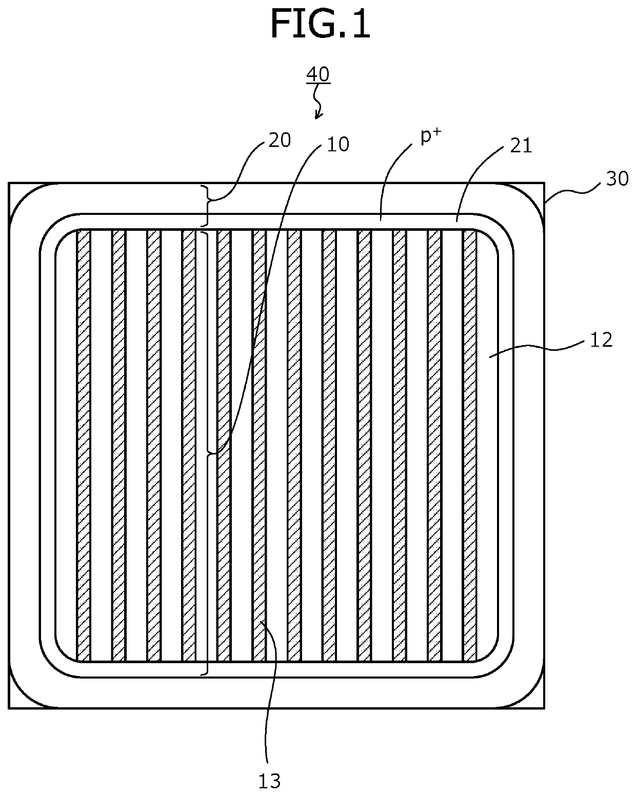
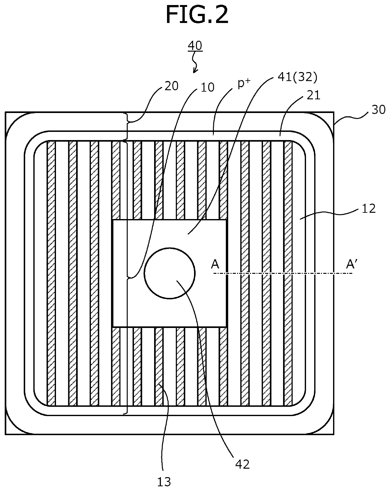
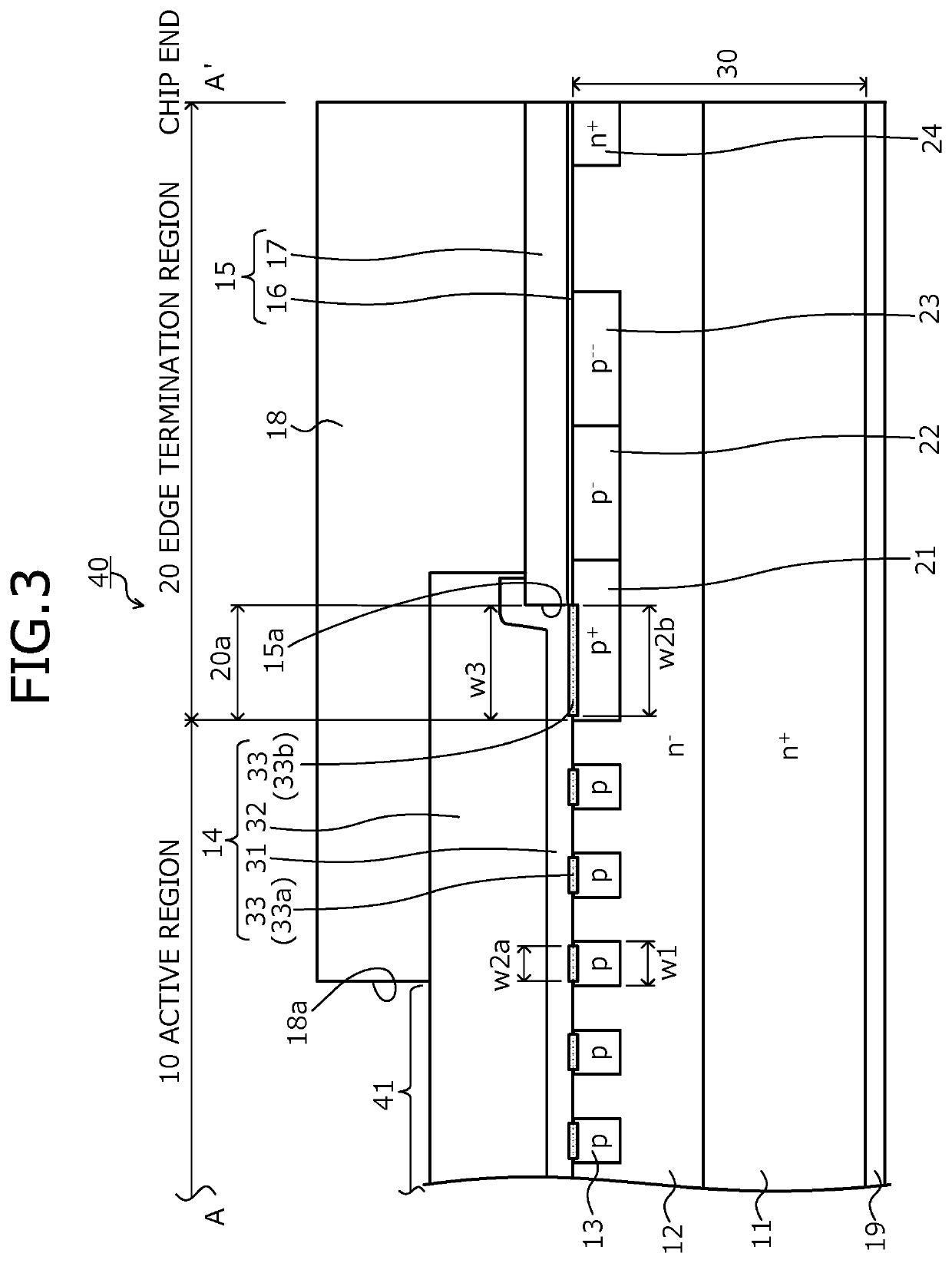
[0094]A silicon carbide semiconductor device 40 and depicted in FIGS. 1 and 2 is a silicon carbide diode having in an active region 10, at the front side of the semiconductor substrate 30, a SBD structure configured by Schottky junctions between a front electrode (first electrode) 14 (refer to FIG. 3) and an n−-type drift region (first-conductivity-type region) 12, and a JBS structure configured by pn junctions between the p-type regions 13 and the n−-type drift region 12.
[0095]The n−-type drift region 12 and the p-type regions 13 are disposed substantially evenly and substantially uniformly at a surface of the active region 10. The n−-type drift region 12 and the p-type regions 13, for example, are disposed in a striped pattern extending in a same direction parallel to the front surface of the semiconductor substrate 30 and are disposed in contact with one another and repeatedly alternate one another along a width direction that is orthogonal to a longitudinal direction along whic...
third embodiment
[0182]Therefore, while not depicted, a layout of the first nickel silicide films that form an ohmic contacts with the p-type regions 72, 74 is a same as the layout of the p-type regions 72, 74. In the third embodiment, in the p-type regions 72, 74, a junction area with the first nickel silicide film is greatest directly beneath a bonding part between the front electrode and a wire (not depicted, corresponds to reference numeral 42 in FIG. 2), and with increasing distance of the disposal position from the bonding part of the front electrode and the wire, the junction area with the first nickel silicide film decreases.
[0183]In particular, in the silicon carbide semiconductor device 70 according to the third embodiment depicted in FIG. 20, for example, directly beneath the bonding part (center of the active region 10) of the front electrode and the wire, a p-type region 71 is disposed in a substantially rectangular shape. The p-type regions 72 configuring the JBS structure are disposed...
second embodiment
[0199]In the second reference example, the nickel silicide films 33′ formed so that the silicon concentration of the silicon film 53′ of the metal material film 52′ is less than 1 wt % are depicted in FIG. 27. The nickel silicide films 33′ formed with the silicon concentration of the silicon film 53′ of the metal material film 52′ being set at 1 wt %, which is within the suitable range of the silicon concentration of the aluminum-silicon film of the metal material film 52 used in the method of manufacturing the silicon carbide semiconductor device described above are depicted in FIG. 28.
[0200]As depicted in FIG. 27, it was confirmed that when the silicon concentration of the silicon film 53′ of the metal material film 52′ is set to be less than 1 wt %, the silicide reaction between the semiconductor substrate 30′ and the nickel film 54′ progresses, whereby the excess carbon 34a′ (hatched part) leftover in the semiconductor substrate 30′ is deposited as a layer in the nickel silicid...
PUM
 Abstract
Description
Claims
Application Information
 - R&D Engineer
- R&D Manager
- IP Professional
- Industry Leading Data Capabilities
- Powerful AI technology
- Patent DNA Extraction
Browse by: Latest US Patents, China's latest patents, Technical Efficacy Thesaurus, Application Domain, Technology Topic, Popular Technical Reports.
© 2024 PatSnap. All rights reserved.Legal|Privacy policy|Modern Slavery Act Transparency Statement|Sitemap|About US| Contact US: help@patsnap.com