
Direct Exposure Device for the Direct Exposure of Solder Resists in a 2-Dimensional, Quickly Temperature-Controlled Environment

a technology of direct exposure and solder resist, which is applied in the direction of double exposure, circuit masks, instruments, etc., can solve the problems of high power loss, indefinable non-linear scaling of masks, and image defects of solder resists

Active Publication Date: 2021-03-25
LIMATA
View PDF0 Cites 1 Cited by
  • Summary
  • Abstract
  • Description
  • Claims
  • Application Information

AI Technical Summary

Benefits of technology

The patent describes an optical system that can adjust the performance of a light source and laser diode in real-time, allowing for better imaging of edges and oblique paths. The system also allows for the adjustment of the maximum IR performance intensity onto the substrate, regardless of its thickness, and can regulate the "catalyst effect" on the copper area. The adjustment can be done manually or with the aid of a motorized system.

Problems solved by technology

A disadvantage of these high-energy UV light sources was high power losses.
Hence, an indefinable non-linear scaling of the mask ensues and thus imaging defects of the solder resist image ensue.
The structure size, for example, changes and entails defects in the design of the printed circuit board; furthermore, the non-linear scaling adversely affects the fitting accuracy of the solder resist to be exposed with respect to the already structured track.
The direct exposure of solder resists in the prior art is performed using UV lasers or UV light-emitting diodes, which can only achieve a high output power in the image field of the exposure when they are numerously cascaded.
In particular, it is known from the prior art that the output power of one individual UV LED or laser diode is too low for achieving rapid UV polymerization of the solder resist.
However, since an individual laser diode is expensive, the UV direct exposure becomes too expensive and thus no longer economical in the case of too high cascading.
Besides, other lasers emitting light in the UV range are also expensive so that an exposure to UV light having a high light intensity is either expensive and rapid or cheap and slow.
Moreover, not all direct exposure technologies are able to transfer unlimited light power into the image plane since power loss in optical elements may entail high temperature influences and thus a short lifetime of the components.
Generally, some manufacturers of solder resists recommend that the maximum temperature during the exposure should not exceed 35° C. Moreover, in a precision tool, such as a direct exposure device, a general heat introduction necessarily entails that the environmental temperature is heated as well and thus entails undesired thermal expansion effects in the device itself, e.g. the setup of the direct exposure device which comprises, e.g., metal or aluminum parts.
Also the general heating of the printed circuit board, onto which the solder resist to be structured is applied, by means of heating elements likewise leads to undesired expansion effects.
However, this is only possible for a process or situation which is stable in terms of temperature and involves deviations of only a few degrees.
Moreover, the all-over heating operation will considerably depend on the material thickness as well as the copper thickness so that a preliminary examination of the exact board parameters would be necessary, which in practice with setup tolerances of the galvanic processes partly are too high in the manufacturing tolerances.

Method used


Image

  • Direct Exposure Device for the Direct Exposure of Solder Resists in a 2-Dimensional, Quickly Temperature-Controlled Environment
  • Direct Exposure Device for the Direct Exposure of Solder Resists in a 2-Dimensional, Quickly Temperature-Controlled Environment
  • Direct Exposure Device for the Direct Exposure of Solder Resists in a 2-Dimensional, Quickly Temperature-Controlled Environment

Examples


Embodiment Construction

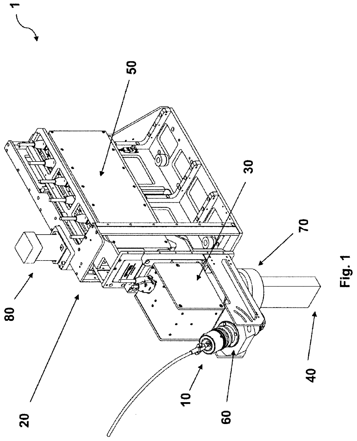
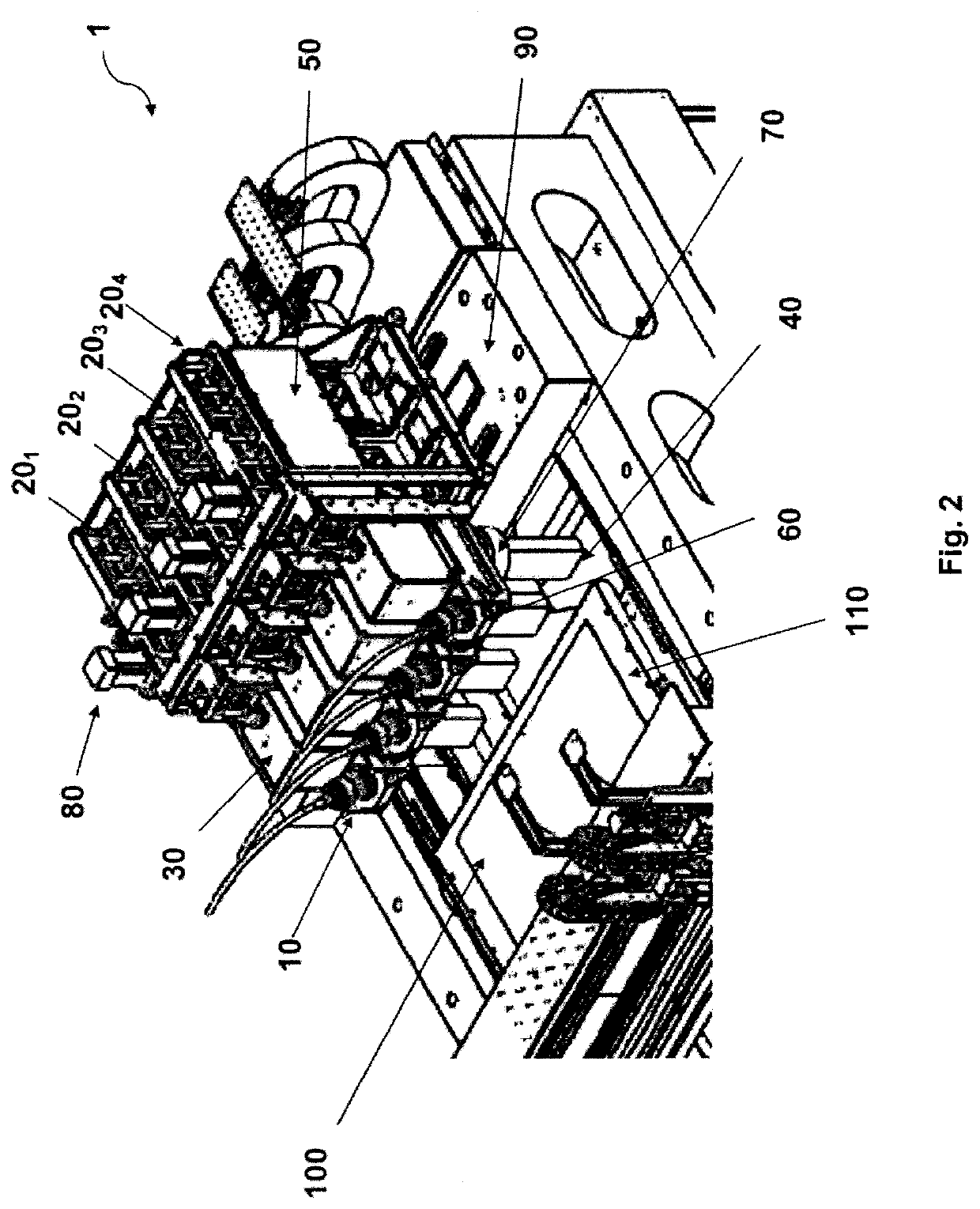
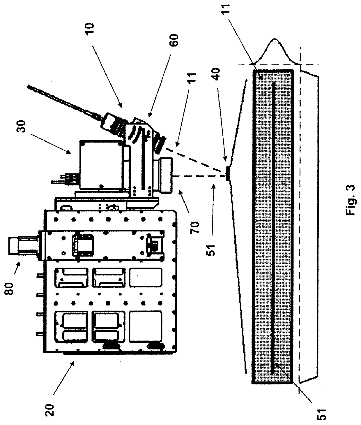
[0086]FIG. 1 shows a perspective view of a direct exposure device 1 (in the following also referred to as lithographic exposure device) comprising an exposure device 20 and an external heat source device 10. The heat source device 10 can be mounted to the exposure device 20, for example, via an adjustment device 60.

[0087]This assembly preferably comprises a laser diode module comprising coupling optics 50 with transmitting laser light beams in the ultraviolet spectral range of 350 nm-450 nm.

[0088]Preferably the coupling takes place within the laser module and is performed by optical elements from the prior art. To this end, for example, pole cubes and semipermeable mirrors as well as other combination optics are used. Preferably, lasers having discrete single-mode wavelengths with different main maxima are coupled or combined in the coupling optics 50. For example, the light beams of three laser sources with main maxima at about 375 nm, 390 nm and 405 nm can be coupled.

[0089]The ind...


PUM

PropertyMeasurementUnit
wavelengthsaaaaaaaaaa
temperatureaaaaaaaaaa
sizeaaaaaaaaaa

Abstract

The invention generally relates to an exposure device, in particular an exposure device for exposing and structuring a substrate coated with a solder resist, as well as the corresponding method for exposure with the exposure device according to the invention. In particular, the invention relates to an exposure device having at least one light beam, formed preferably by two or more laser beams of different UV wavelengths, which is deflected relative to the substrate by a variable deflection device, in order to generate structures on the substrate. In particular, the light beam is superimposed, spatially in the image plane and temporally in the exposure, by a spatially limited, high-energy, preferably externally mounted heat source, wherein preferably infrared laser diodes having linear optics are used.

Description

FIELD OF THE INVENTION[0001]The present invention generally relates to an exposure device, in particular a direct exposure device or lithographic exposure device for directly exposing a substrate coated with a photosensitive layer in order to manufacture a printed circuit board, i.e., a PCB, or a photo-etched part, and to the corresponding method for exposing substrates with the direct exposure device according to the present invention. In particular, the invention relates to an exposure device having at least one UV light beam which is deflected relative to the substrate by a variable deflection device in order to generate structures in the photosensitive layer. Preferably, the light beam is formed by two or more laser beams having different UV wavelengths. In particular, the light beam is superimposed, in the image plane in terms of space and in the exposure in terms of time, by a spatially limited, preferably externally mounted heat source, wherein preferably infrared laser diode...

Claims


Application Information

Patent Timeline
Patent Type & Authority Applications(United States)
IPC IPC(8): H05K3/06H05K3/00G03F7/20
CPCH05K3/06H05K2203/108G03F7/2053H05K3/0082H05K3/064H05K2203/0505H05K2203/107G03F7/168G03F7/2004
Inventor NAGEL, MATTHIAS
Owner LIMATA
Learn More