Process environment for inorganic resist patterning

a technology of resist patterning and processing environment, which is applied in the field of processing of radiation-sensitive organometallic patterning compositions, can solve the problems of many of these materials being susceptible to environmental effects

Pending Publication Date: 2021-09-02
TOKYO ELECTRON LTD
View PDF8 Cites 2 Cited by
  • Summary
  • Abstract
  • Description
  • Claims
  • Application Information

AI Technical Summary

Benefits of technology

[0078]This example illustrates the effect of controlled processing delays on the patterning performance of an organotin photoresist.

Problems solved by technology

Despite these advantages, it is known that many of these materials are susceptible to environmental effects such as humidity or composition of atmospheres the wafer is exposed to throughout the multi-step manufacturing process.

Method used


Image

  • Process environment for inorganic resist patterning
  • Process environment for inorganic resist patterning
  • Process environment for inorganic resist patterning

Examples


example 1

Gas Concentration Effects on Processing

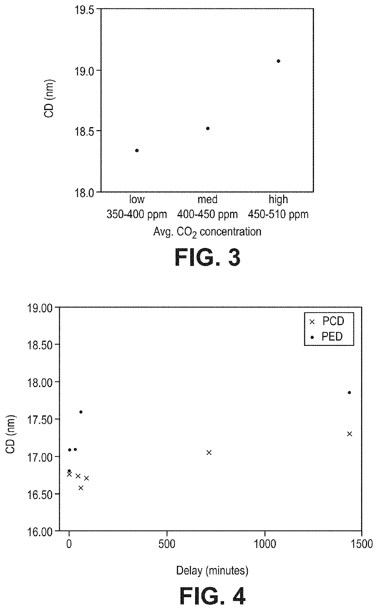
[0071]This example illustrates the effect that the concentration of a reactive gas, in this case carbon dioxide, can have on patterning performance of an organotin photoresist.

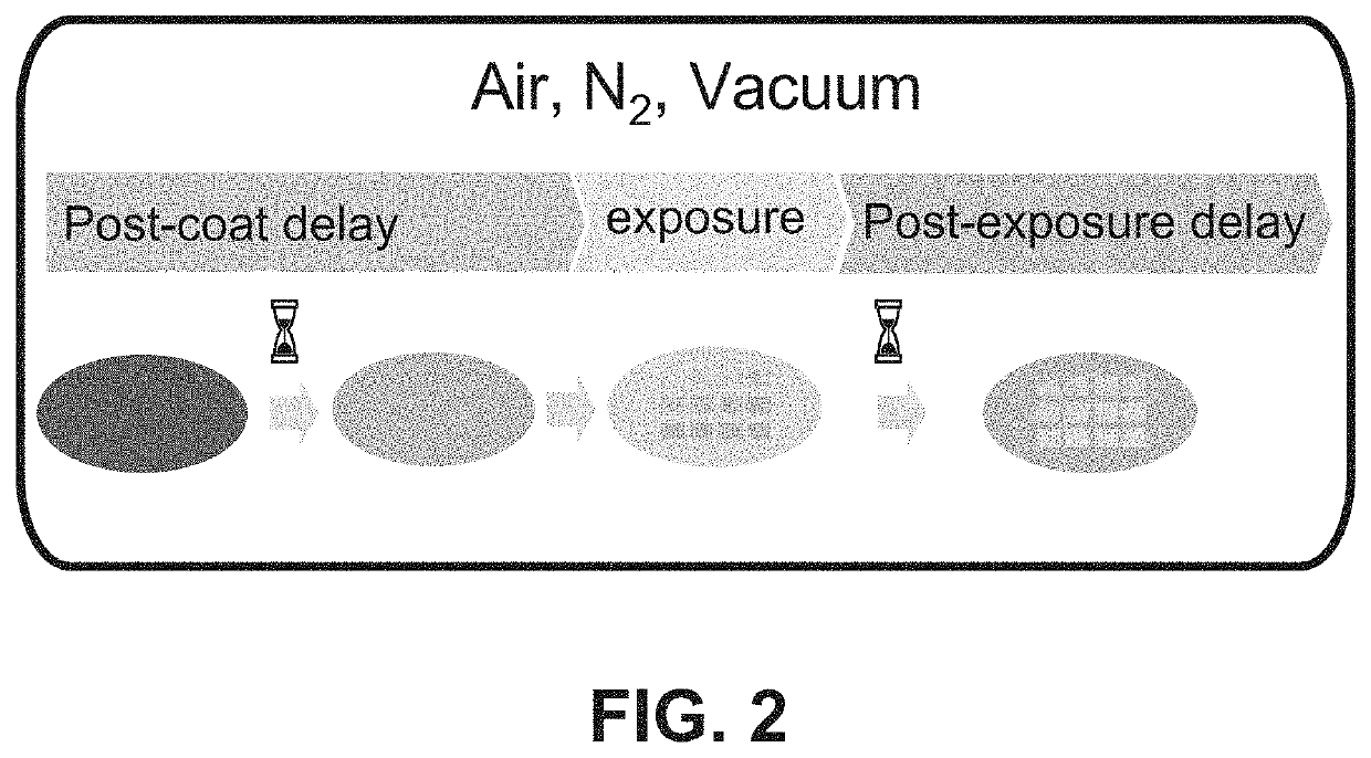
[0072]General Coating and Processing Steps

[0073]Silicon wafers having a 10 nm layer of spin-on-glass (SOG) were used as the substrates. The wafers were coated with approximately 20 nm of organotin photoresist. The wafers were then baked at 100° C. for 60 s, exposed to EUV radiation on an ASML NXE3400 exposure tool at 47.1 mJ / cm2, subsequently baked at 170° C. for 60 seconds, developed in 2-heptanone, and subject to a final bake at 150° C. for 60 seconds.

[0074]Processing with Reactive Gas

[0075]Three wafers were each individually processed under atmospheres having differing levels of CO2 ranging from a low of 354 ppm to a high of 506 ppm. The atmospheric components were constant throughout the processing for each individual wafer, except for during exposure, which was condu...

example 2

Processing Delays

[0078]This example illustrates the effect of controlled processing delays on the patterning performance of an organotin photoresist.

[0079]Two sets of wafers were coated and processed as described in the General Coating and Processing Steps in Example 1 with each set being subjected to delays at different points in the processing. One set of wafers was processed with a variable post-coat delay (PCD) wherein the substrate was coated, and then each wafer held in an ambient air atmosphere for a different amount of time, indicated as the delay. The post-coat delay (PCD) samples are shown in FIG. 4 with the “X” data labels. A second set of wafers was processed as normal through radiation patterning with EUV radiation, and then each wafer was processed with a variable post-exposure delay (PED) wherein each was held in ambient air atmosphere for a different amount of time (delay) prior to undergoing a post-exposure bake. The post-exposure delay (PED) samples are shown in FI...

example 3

tmosphere Effects During Exposure

[0081]This example illustrates the effect that a radiation exposure in a nitrogen atmosphere versus in an air atmosphere can have on patterning performance of an organotin photoresist.

[0082]Thin films for contrast curves were deposited on silicon wafers (150-mm diameter) having a native-oxide surface. A wafer stack was prepared by first depositing an approximately 60 nm bottom anti-reflection coating (BARC) (DUV46M, Brewer Science) by spin coating at 1300 rpm and then coating with approximately 20 nm of organotin photoresist, by spin coating the organotin solution at 1000 rpm. The wafers were then baked at 100° C. for 2 minutes. Exposure to 254 nm radiation was conducted by using a UVP UV Transilluminator operated at a laser power of 4.7 mW / cm2, configured within an in-house UV exposure system, as shown in FIG. 5, for 3 minutes. FIG. 5 illustrates in-house UV exposure system 200 having UV source 202, which was a UVP UV Transilluminator, upon which is...


PUM

PropertyMeasurementUnit
thicknessaaaaaaaaaa
pressureaaaaaaaaaa
pressureaaaaaaaaaa

Abstract

The processing of radiation patternable organometallic coatings is shown to be improved through the appropriate selection of post processing conditions between coating and development of the pattern. In particular, a coated wafer can be subjected to process delays to allow aging of the coating at various process points, in particular following irradiation. Process delays can be combined and interspersed with heating steps. The atmosphere above the coated wafer at various process steps can be adjusted to obtain desired improvements in the development of the pattern. Reactive gases can be beneficial with respect to improvement of coating properties.

Description

CROSS REFERENCE TO RELATED APPLICATIONS[0001]This application claims priority to copending U.S. provisional patent application 62 / 984,023, filed Mar. 2, 2020 to Telecky et al., entitled “Process Environment For Inorganic Resist Patterning,” incorporated herein by reference.FIELD OF THE INVENTION[0002]The invention related to the processing of radiation sensitive organometallic patterning compositions, in particular organo tin oxide hydroxide based compositions, with respect to the deposition through development of a pattern.BACKGROUND OF THE INVENTION[0003]Semiconductor manufacturing demands both high performance and high reproducibility of the materials and processes that comprise the fabrication of semiconductor devices. During high-volume manufacturing, for example, it is desirable for a lithography process to yield features of identical size and shape in a repeatable fashion across many wafers and across many days and it is therefore desirable that the patterning stability of li...

Claims


Application Information

Patent Timeline
Patent Type & Authority Applications(United States)
IPC IPC(8): G03F7/38G03F7/004
CPCG03F7/38G03F7/0042
Inventor TELECKY, ALAN J.STOWERS, JASON K.KESZLER, DOUGLAS A.MEYERS, STEPHEN T.DE SCHEPPER, PETERCASTELLANOS ORTEGA, SONIAGREER, MICHAELLOUTHAN, KIRSTEN
Owner TOKYO ELECTRON LTD
Why Eureka
Try Eureka