
Doped semiconductor nanocrystals, method for preparing same and uses thereof

a technology of semiconductor nanocrystals and doped semiconductors, which is applied in the direction of crystal growth process, polycrystalline material growth, luminescent compositions, etc., can solve the problem of difficult use, large stokes shift, and insufficient stokes shift to avoid losses

Pending Publication Date: 2022-03-03
COMMISSARIAT A LENERGIE ATOMIQUE ET AUX ENERGIES ALTERNATIVES
View PDF1 Cites 0 Cited by
  • Summary
  • Abstract
  • Description
  • Claims
  • Application Information

AI Technical Summary

Benefits of technology

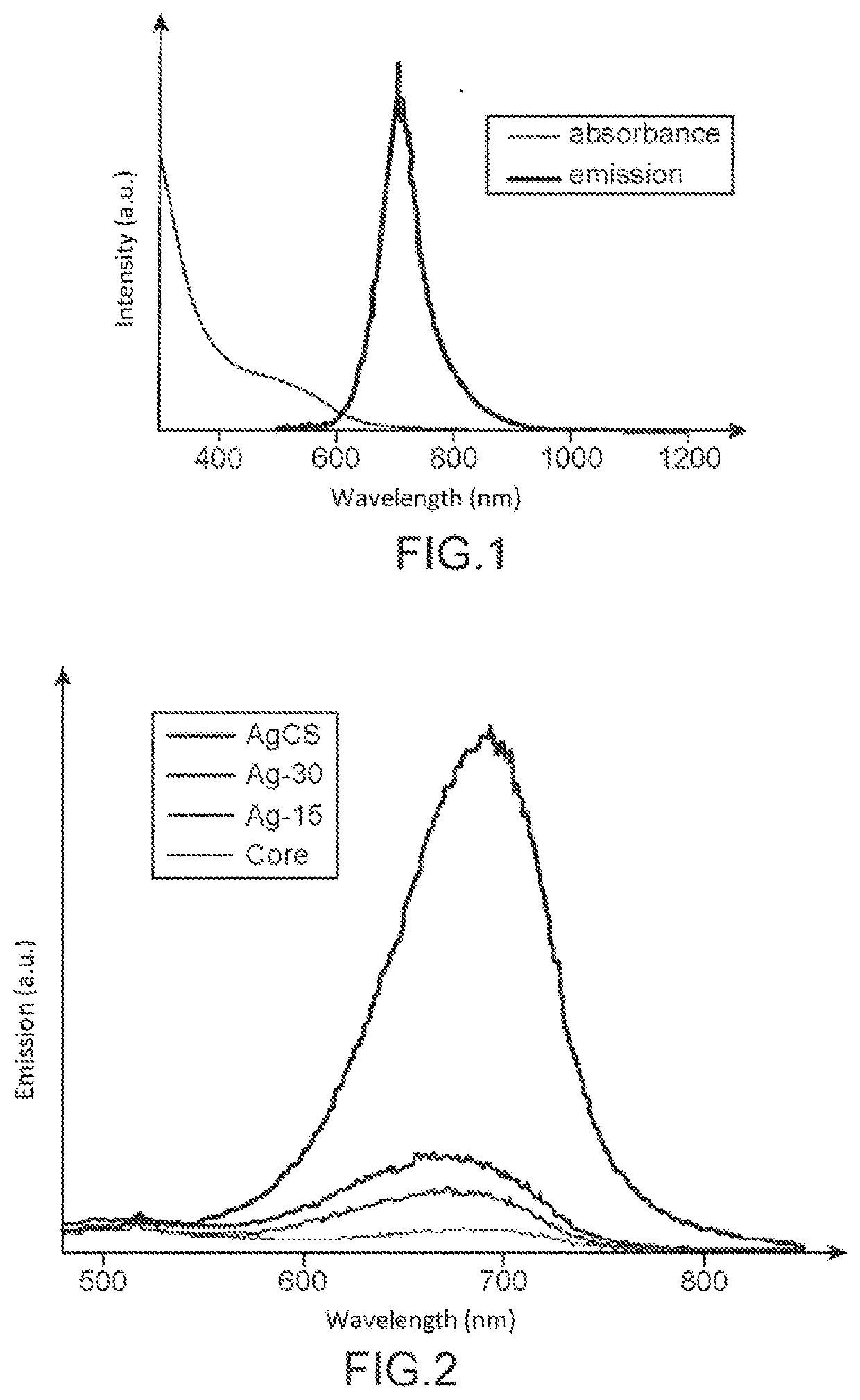
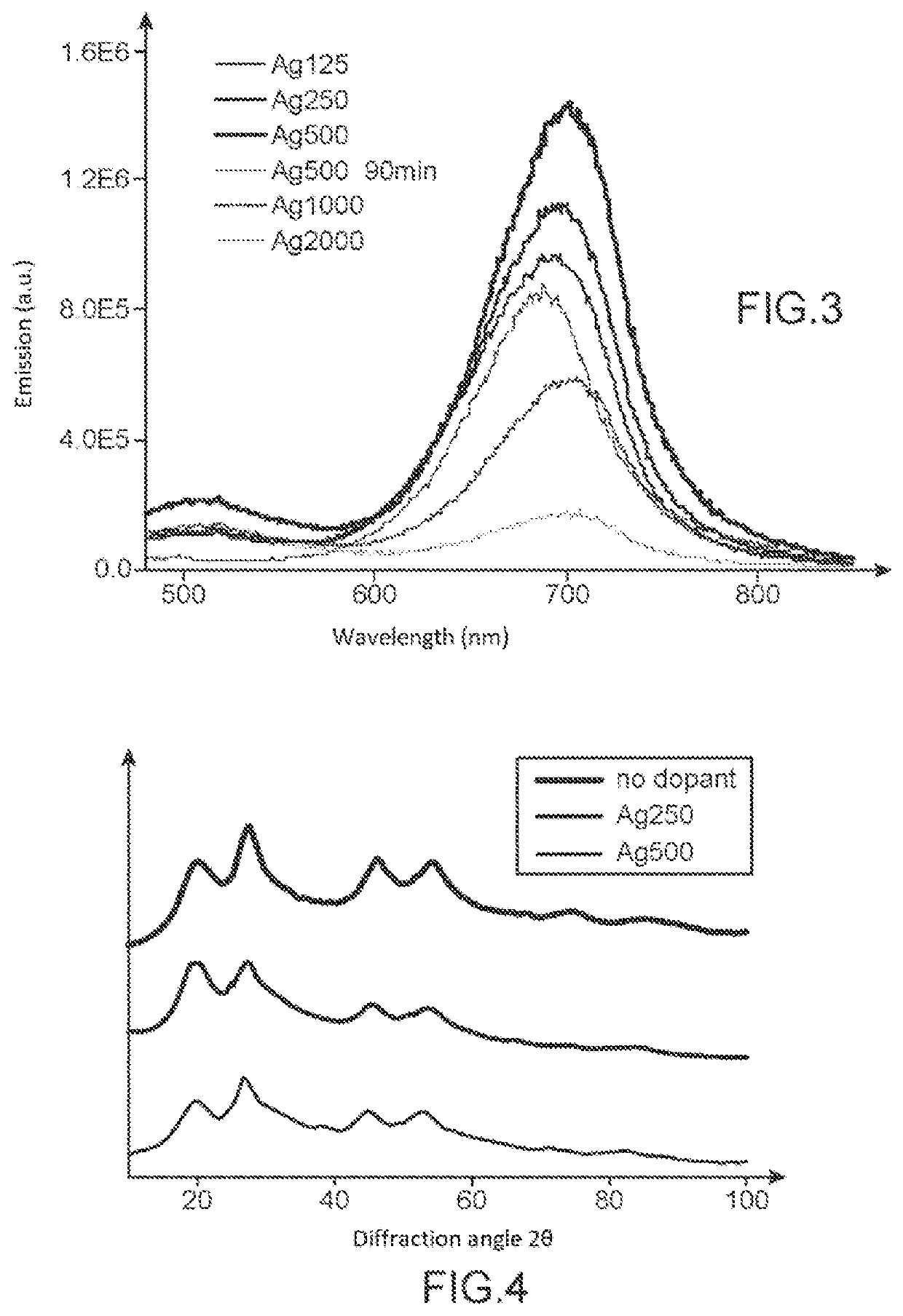
The present invention proposes a new type of semiconductor nanocrystal that is doped with a transition metal and optionally coated with a semiconductor shell. These nanocrystals have improved optical properties, such as a narrow emission profile in the red or near infrared range, a high photoluminescence quantum yield, and an absence of overlap between the absorption and emission spectra (Stokes shift). The nanocrystals can be used in various applications, such as light-emitting diodes, photovoltaics, sensors, and biological imaging. The invention also provides a method for preparing these nanocrystals and their use in various applications.

Problems solved by technology

However, the Stokes shift is not large enough to avoid losses caused by reabsorption.
The latter are difficult to use in the envisaged applications because of very broad emission in the red range and poorly defined absorption.
This introduction leads to a broadening of the emission profile in the red range, which is contrary to the desired optical properties.

Method used


Image

  • Doped semiconductor nanocrystals, method for preparing same and uses thereof
  • Doped semiconductor nanocrystals, method for preparing same and uses thereof
  • Doped semiconductor nanocrystals, method for preparing same and uses thereof

Examples


Embodiment Construction

[0142]I. Material and Methods

[0143]I.A. Preliminary Remarks

[0144]All the syntheses are carried out in an inert atmosphere using argon gas.

[0145]For the characterisations, the UV-visible absorption spectra were measured on a HP8420A spectrometer (spectral range in wavelength: 190 nm to 820 nm, resolution 2 nm), the photoluminescence spectra were acquired with a HORIBA Fluorolog iHR320 spectrometer. For these spectroscopic measurements, the colloidal solutions of nanocrystals diluted in hexane were placed in small quartz cells with an optical path of 1 cm. The fluorescence quantum yields at ambient temperature were obtained by comparing the emission intensity—spectrally integrated—of the dispersion of nanocrystals in the hexane with that of a solution of rhodamine 6 G in ethanol, the two solutions having the same optical density (<0.03) at the excitation wavelength (490 nm). The X-ray diffractograms were obtained on a Philips Panalytical device, using a source of copper, at 40 kV and ...


PUM


Abstract

A set of nanocrystals comprising a semiconductor comprising A representing a metal or metalloid in the +III oxidation state and B representing an element in the −III oxidation state, the nanocrystals being doped, on average per nanocrystal, by an atom of C chosen from the transition metals in the +I or +II oxidation state and various uses thereof.

Description

DESCRIPTIONTechnical Field[0001]The present invention relates to the technical field of luminescent semiconductor nanocrystals and in particular doped semiconductor nanocrystals.[0002]More particularly, the present invention proposes nanocrystals based on a type III-V semiconductor weakly doped with a transition metal in the +I or +II oxidation state, said nanocrystals being optionally coated with a shell of a semiconductor, identical to or different from the semiconductor of said nanocrystals.[0003]The present invention also relates to a method for preparing such nanocrystals and their various uses. Indeed, the field of application of these nanocrystals includes, for example, light-emitting diodes, photovoltaic cells, the fluorescent marking of chemical molecules, in particular for anti-counterfeiting purposes and the fluorescent labelling of biological molecules, in particular, for biological imaging and detection.Prior Art[0004]In a general way, nanoparticles are of great interes...

Claims


Application Information

Patent Timeline
IPC IPC(8): C09K11/70H01L33/50C30B7/14H01L31/055C30B29/40
CPCC09K11/70H01L33/502C30B29/40H01L31/055C30B7/14C01B25/088B82Y40/00B82Y30/00Y02E10/52
Inventor AKDAS, TUGCEREISS, PETER
Owner COMMISSARIAT A LENERGIE ATOMIQUE ET AUX ENERGIES ALTERNATIVES
Learn More