A method for preparing a cross-size micro-nano structure array

Pending Publication Date: 2022-10-27
SUZHOU UNIV
View PDF0 Cites 0 Cited by
  • Summary
  • Abstract
  • Description
  • Claims
  • Application Information

AI Technical Summary

Benefits of technology

[0021]The beneficial effect of the invention is:
[0022]1. The method for preparing a cross-size micro-nano structure array of the invention uses multi-beam laser interference to assist electrochemical dissolution or electrochemical deposition, and controls physical fields such as temperature field and electric field in a specific area on the surface of the material by using interference light field to control the electrochemical dissolution or electrochemical deposition speed of the workpiece material in this area, and combined with the high localization characteristics of ultrashort pulse electrochemical machining, achieves the preparation of large-area metal micro-nano structure arrays without masks.
[0023]2. The fine trimming wire electrode is used as the tool electrode, which solves the problem of low output power of the existing ultrashort pulse power supply. During the machining process, the trimming wire electrode removes or electrochemically deposits the workpiece material layer by layer in a reciprocating scanning motion, thereby improving the machining accuracy of the micro-nano structure array.
[0024]3. During the machining process, since there are

Problems solved by technology

However, as the feature size of the device decreases, the surface forces that are usually ignored at the macro scale, such as van der Waals force, adhesive force, electrostatic force, and capillary force, have become the main factors restricting the normal operation of micro components or systems at the micro scale.
However, the traditional micro-nano processing technologies, such as micro-milling, laser processing, abrasive gas jet, EDM and mask electrochemical machining, etc., although they can be used for arrays of metal surface microstructures, they all have certain limitations.
It is difficult to achieve the preparation of microstructure arrays with feature sizes below a few microns.
When the characteristic parameters of the microstructure need to be changed, the mask must be remade, which not only causes a waste of materials, but also prolongs the process cycle.
When the characteristic size of the pattern structure is reduced to about 10 microns, it is difficu

Method used


Image

  • A method for preparing a cross-size micro-nano structure array
  • A method for preparing a cross-size micro-nano structure array
  • A method for preparing a cross-size micro-nano structure array

Examples


Example

The First Embodiment

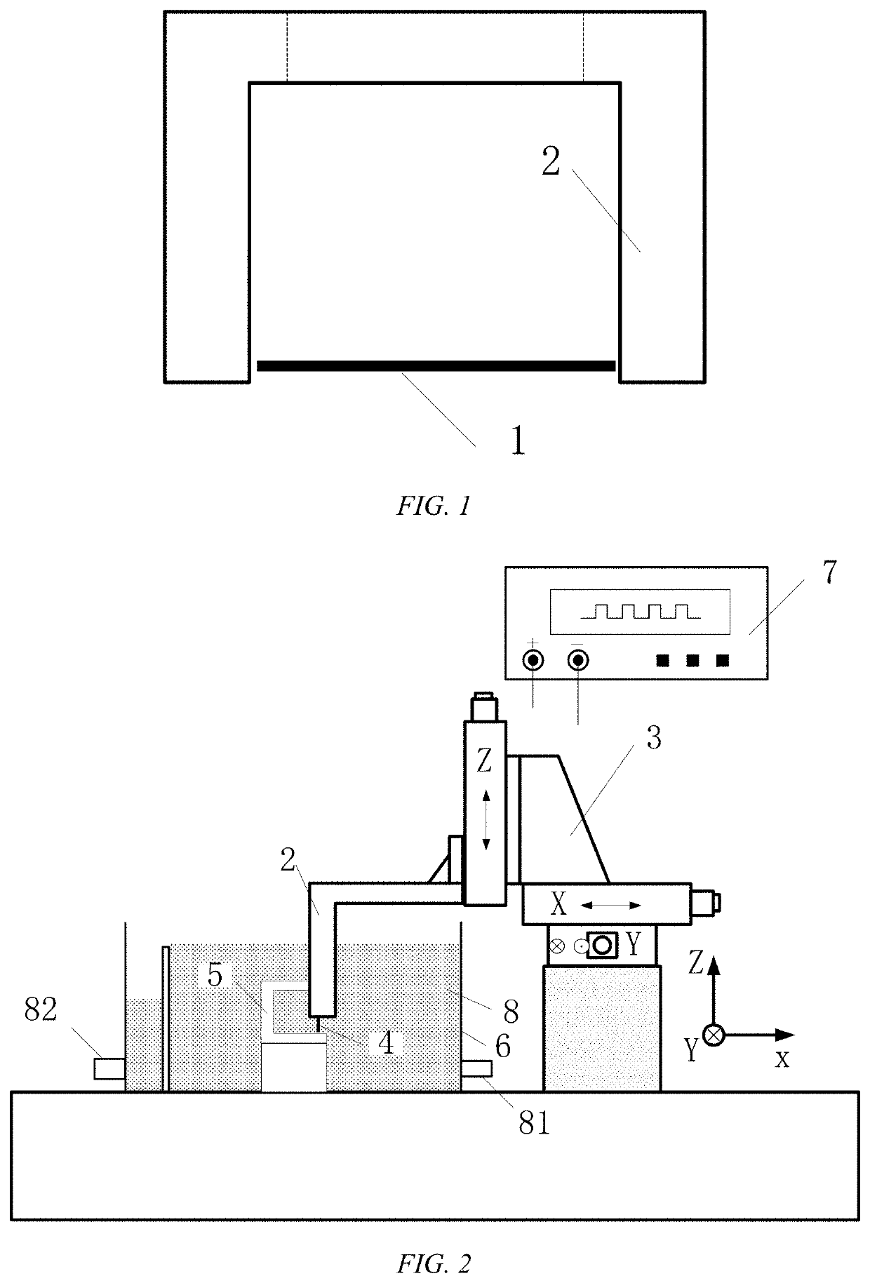
[0059]Step 1: Online Preparation of the Trimming Wire Electrode 10

[0060]Please refer to FIG. 1 to FIG. 4, install the metal tungsten wire 1 with a diameter of 50 μm in the cathode fixture 2 with a tension of 2N, and install the cathode fixture 2 on the motion platform 3; Install the electrode fixture 5 equipped with a fine tungsten wire 4 with a diameter of 10 μm in the electrolyte tank 6; the positive electrode of the ultrashort pulse power supply 7 is connected with the metal tungsten wire 1, and the negative electrode is connected with the fine tungsten wire 4; The KOH electrolyte 8 with a concentration of 0.1 mol / L is placed in the electrolyte tank 6 and make the electrolyte 8 completely flood the metal tungsten wire 1; Set the output voltage amplitude (Z) of the ultra-short pulse power supply 7 to 5V, the pulse period (P) to 1 us, and the pulse width (ton) to 100 ns. The initial machining gap 9 between the metal tungsten wire 1 and the fine tungsten wire 4 i...

Example

The Second Embodiment

[0063]Step 1: Online Preparation of the Trimming Wire Electrode 10

[0064]This step is the same as the preparation method in The first embodiment, and will not be repeated here.

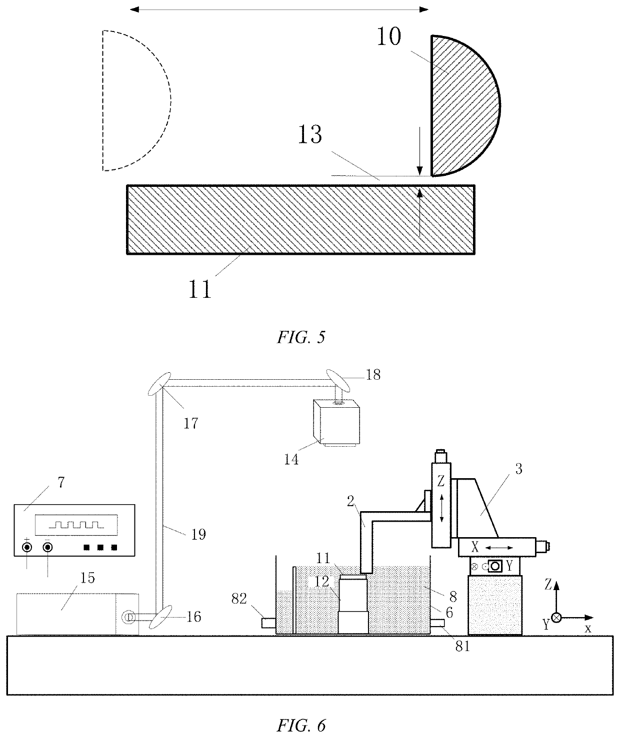
[0065]Step 2: Laser Interference-Electrochemical Deposition is Performed on the Surface of the Workpiece 11 to Obtain a Micro-Nano Structure Array

[0066]Take a copper sheet with a size of 10 mm*10 mm*2 mm as the workpiece 11, and install it in the electrolyte tank 6 through the workpiece fixture 12; The prepared trimming wire electrode 10 is moved to the top of the workpiece 11 through the moving platform 3, and the gap 13 between the trimming wire electrode 10 and the workpiece 11 is set to 1 um; The electrolyte tank 6 is filled with the CuSO4 electrolyte 8 with a concentration of 1.5 mol / L; The output mode of the interference beam regulator 14 is set to four-beam interference, The incident angle is 15°, the laser spot size is 15 mm, and the energy density is 1.1 J / cm2; Connect the negative...


PUM


Abstract

A method for preparing a cross-dimension micro-nano structure array includes: S1. providing a workpiece immersed in the electrolyte as the first electrode, providing a trimming wire electrode as the second electrode and setting it above the workpiece, providing an interference beam adjuster and outputting multi-beam laser interference to irradiate the surface of the workpiece; S2. The power supply between the first electrode and the second electrode forms a loop, and drives the trimming wire electrode to reciprocate relative to the workpiece, and the workpiece undergoes electrochemical dissolution or electrochemical deposition at the corresponding position of the trimming wire electrode, and form a micro-nano structure array without a mask, and solves the problem of low output power of the existing ultrashort pulse power supply, improves the processing accuracy of the micro-nano structure array, does not require electrolyte for high-speed flow, and improves system safety and reduce the cost.

Description

[0001]This application claims the benefit of priority from the Chinese patent application No. 202011284967.9, filed on Nov. 17, 2020, which is incorporated herein by reference in its entirety.FIELD OF THE INVENTION[0002]The invention relates to a method for preparing a cross-size micro-nano structure array, belonging to the field of precision and micro-manufacturing.BACKGROUND OF THE INVENTION[0003]Precision and miniaturization are the mainstream development directions of modern industrial, civilian and military products. However, as the feature size of the device decreases, the surface forces that are usually ignored at the macro scale, such as van der Waals force, adhesive force, electrostatic force, and capillary force, have become the main factors restricting the normal operation of micro components or systems at the micro scale. In recent years, surface microtexturing technology, which uses micro-nano processing technology to construct a certain shape, size and arrangement of m...

Claims


Application Information

Patent Timeline
IPC IPC(8): B23H5/00B23H3/02B23H9/00B23K26/36B23K26/00B23K26/06
CPCB23H5/00B23H3/02B23H9/008B23K26/36B23K26/0093B23K26/0604B23H2300/10B23H5/06B23H3/04B23H7/08B23H7/02
Inventor HE, HAIDONGXI, ZIJIEWANG, CHUNJUSUN, LININGNING, XUEZHONG
Owner SUZHOU UNIV
Why Eureka
Try Eureka