Field effect transistor with a negative capacitance gate structure

a field effect transistor and gate structure technology, applied in the direction of diodes, semiconductor devices, electrical apparatus, etc., can solve the problems of limiting the continued growth of integrated circuits, increasing complexity of electronic circuits, and difficulty in miniaturizing semiconductor circuits

Pending Publication Date: 2022-10-27
TERRA QUANTUM AG
View PDF0 Cites 0 Cited by
  • Summary
  • Abstract
  • Description
  • Claims
  • Application Information

AI Technical Summary

Benefits of technology

[0010]The field-effect transistor with the negative capacitance gate structure may provide an enhanced switching speed. The field-effect transistor with the negative capacitance gate structure may also provide an improved energy efficiency. Consequently, the field-effect transistors with the negative capacitance gate structure may operate with the reduced energy dissipation and generate less waste heat, which may further improve the performance of the field-effect transistor. The field-effect transistor with the plurality of topological domains may provide a stable and reversible negative capacitance. The field-effect transistors with the plurality of topological domains may operate with reduced or even a negligible hysteresis of a voltage at the channel with respect to a voltage applied to the top electrode.
[0031]A reference line may be shifted with respect to the shortest separation line, and in particular may extend in parallel to the shortest separation line and at least partially in a surface defined by the cross-sectional area. A length of the reference line within the cross-sectional area may be shorter than a length of the shortest separation line within the cross-sectional area, and the length of the reference line within the cross-sectional area may differ from the length of the shortest separation line within the cross-sectional area by a difference which increases with increasing distance between the reference line and the shortest separation line in a vicinity of the shortest separation line. The shortest separation line may provide an image for the at least one topological domain wall. The difference between the length of the shortest separation line and the reference line may express an enhanced reliability and robustness of the negative capacitance.
[0053]Embodiments with exactly two topological domains may give a high level of control over the formation of the topological domain wall, in particular the controlled formation of the topological domain wall at a position close of the shortest separation line.
[0075]The first structure may be formed on one part of a semiconductor substrate, and the second structure may be formed on a different part of the semiconductor substrate. Separating the first structure and the second structure may improve the flexibility of layout design and make a fabrication of a device comprising the field effect transistor more efficient, for example more cost-efficient, and / or easier and / or more reliable.
[0092]In an embodiment, increasing the voltage of the top electrode to a reference value below the gate voltage may generate the same net polarization of the multi-domain element as reducing the voltage of the top electrode to the reference value.
[0094]With particular reference to causing an amplified voltage of the bottom electrode, the amplification effect can be significantly enhanced by means of the additional dielectric element, such as a shell coating, which may tune the total gate capacity to negative but small by its modulus total gate capacitance.

Problems solved by technology

The microelectronics industry is experiencing rapid growth with the trend towards miniaturization, yet with increasing complexity of the electronic circuits.
The ever-increasing power density of integrated circuits may generate waste heat at a high density, threatening to limit the continued growth of integrated circuits in accordance with Moore's Law.
The ongoing miniaturization of the semiconductor circuitry faces challenges due to the power losses in field effect transistors and the resulting generated heat.
However, to this date, not a single material combination nor a single geometry have successfully been shown to realize capacitors with a stable, reversible and hysteresis-free negative capacitance.

Method used


Image

  • Field effect transistor with a negative capacitance gate structure
  • Field effect transistor with a negative capacitance gate structure
  • Field effect transistor with a negative capacitance gate structure

Examples


Embodiment Construction

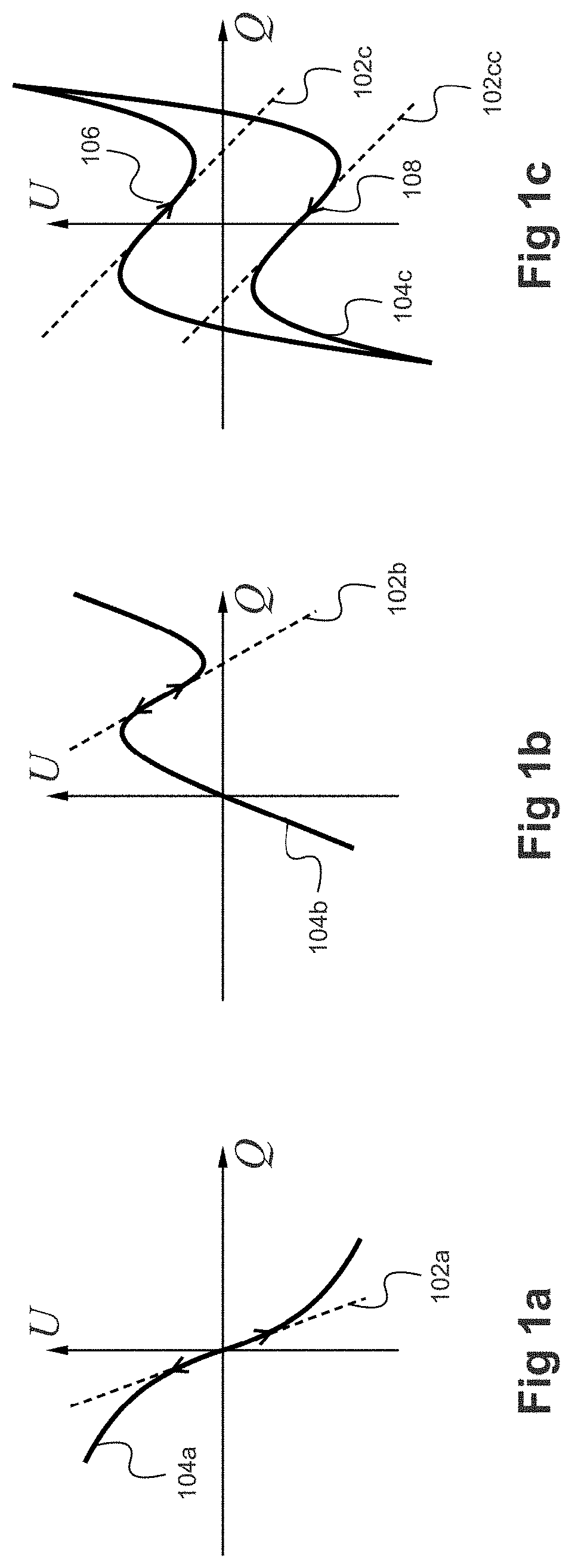
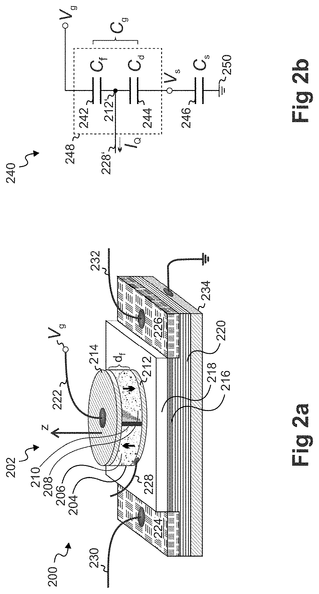
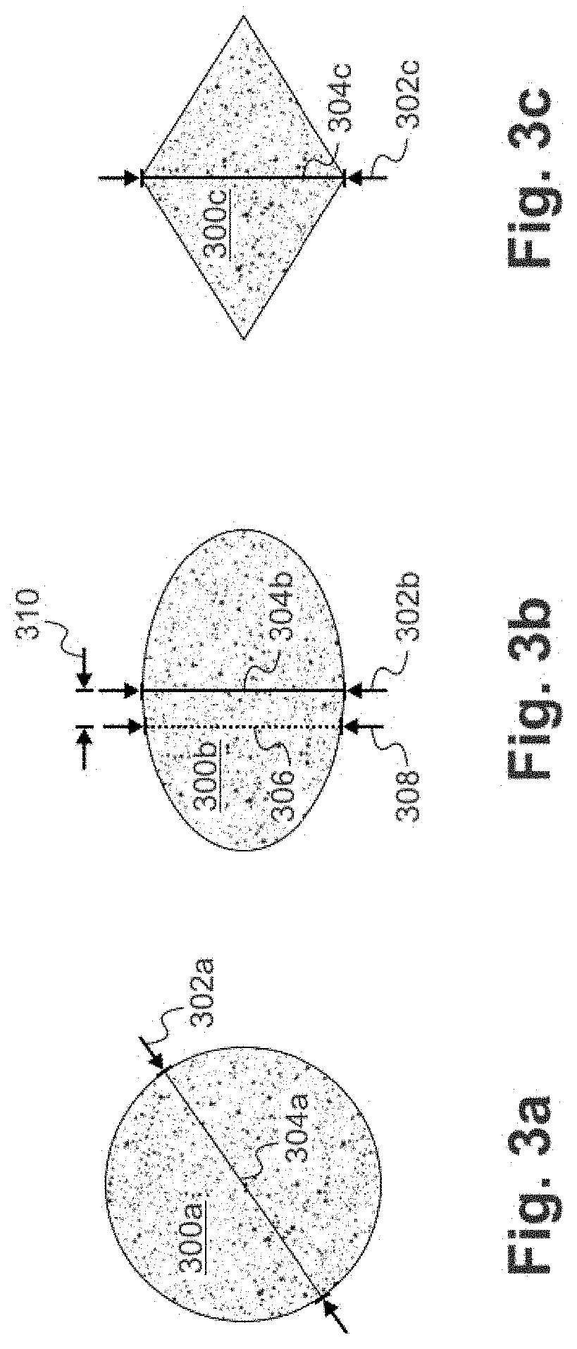
[0111]The following disclosure provides many different embodiments or examples for implementing an electric circuit with the field-effect transistor having a negative-capacitance gate structure to yield improved versatility. Consequently, the present disclosure may widen a capacitance matching window of the field effect transistor. In particular, the present disclosure may implement a negative-capacitance gate structure guaranteeing a reversible, stable static negative capacitance, as opposed to a nonlinear differential capacitance or a transient negative capacitance in the transient dynamical regime.

[0112]Specific examples of components and arrangements are described below to simplify the present disclosure. These are, of course, merely examples that are not limiting. For example, the formation of a first feature over or of a second feature may include embodiments in which the first and second features are formed in direct contact. These features may also include embodiments in whi...


PUM

PropertyMeasurementUnit
widthaaaaaaaaaa
widthaaaaaaaaaa
widthaaaaaaaaaa

Abstract

A field effect transistor has a negative capacitance gate structure. The field effect transistor comprises a channel and a gate dielectric arranged over the channel. The negative capacitance gate structure comprises a bottom electrode structure comprising a bottom electrode, a multi-domain structure, and a top electrode structure. The multi-domain structure comprises a multi-domain element arranged over the bottom electrode, the multi-domain element comprising a plurality of topological domains and at least one topological domain wall. The top electrode structure comprises a top electrode arranged over the multi-domain element. At least a section of the bottom electrode structure of the negative capacitance gate structure is arranged over the gate dielectric and adapted to be coupled to the channel through the gate dielectric.

Description

CROSS-REFERENCE TO RELATED APPLICATIONS[0001]This patent application claims priority to European patent application ser. No. EP21168691.0, filed on Apr. 15, 2021, which is incorporated herein in its entirety by reference.FIELD OF THE DISCLOSURE[0002]The disclosure relates to a field-effect transistor, in particular to a gate structure of a field-effect transistor, and more specifically to a gate structure with a negative capacitance.BACKGROUND OF THE INVENTION[0003]The microelectronics industry is experiencing rapid growth with the trend towards miniaturization, yet with increasing complexity of the electronic circuits. The functional density (i.e., the number of interconnected devices per chip area) is increasing while the geometric size (i.e., the smallest component of circuit) that may be created using a state-of-art fabrication process is decreasing. The ever-increasing power density of integrated circuits may generate waste heat at a high density, threatening to limit the conti...

Claims


Application Information

Patent Timeline
Patent Type & Authority Applications(United States)
IPC IPC(8): H01L29/10H01L29/06H01L29/41H01L29/08
CPCH01L29/1029H01L29/0649H01L29/41H01L29/0847H01L29/78391H01L29/42364H01L29/516H01L27/0629H01L29/40111H01L29/42372
Inventor LUKYANCHUK, IGORTIKHONOV, YURIIRAZUMNAYA, ANNAVINOKOUR, VALERII
Owner TERRA QUANTUM AG
Why Eureka
Try Eureka