Monolithic integrated multiple electronic components internally interconnected and externally connected by conductive side castellations to the monolith that are of varying width particularly monolithic multiple capacitors

a monolithic, multiple capacitor technology, applied in the direction of fixed capacitors, fixed capacitor dielectrics, fixed capacitor details, etc., can solve the problems of inability to meet the requirements of the conventional layout, the difficulty of electrical connection to multiple buried-substrat capacitors is multiplied by, and the effort has essentially come to naugh

Inactive Publication Date: 2000-01-04
DEVOE ALAN D +1
View PDF0 Cites 18 Cited by
  • Summary
  • Abstract
  • Description
  • Claims
  • Application Information

AI Technical Summary

Problems solved by technology

Usually this is needed when internal capacitor arrangements make conventional layouts impossible, or to accommodate existing IC pad locations.
The difficulty of making electrical connections to multiple buried-substrate capacitors are, however, multiplied by the number of such separate connections to be made.
This effort has essentially come to naught.
In the first place, the hole placement, by laser drilling or otherwise, tends to displace the conductive material of the electrodes that are penetrated by the drilling down hole, leaving an insufficient amount of this conductive material at the walls of the bores at (and only at) the regions of the exposed down-hole electrodes so as to permit electrical connection to be reliably made to the electrodes.
Moreover, and equally importantly, it is all but impossible to wick solder into the typically small drilled holes.
Finally, any access to these holes is likely--should an electronic device (an IC) be mounted flush to the multiple capacitor as is commonly desired--severely impeded.
To say that this hand soldering work is delicate and painstaking, and therefore expensive, is an understatement.
Present difficulties in electrically connecting one microminiature component to another is one reason that very, very small electronic items such as hearing aids that fit within the external acoustic meatus, or ear canal tend to be expensive, costing several hundreds and even thousands of dollars U.S. circa 1995.
The previous manner of constructing the pad regions at the top surface of a multiple buried-substrate capacitor is itself quite intricate.
Because each multiple capacitor is very small, its registration for patterning, and its subsequent patterning, are each very difficult.
Although the minute top and bottom surface edge regions where the conductive ink has "rolled over" the edge exhibit excellent solder characteristics, these minute and localized regions are distinctly (i) near the edges of the top and bottom surfaces of the multiple capacitor, only, (ii) are undesirably small, and, as such, (iii) are themselves and without more totally unadaptable to forming some arbitrary pattern of pads at which, and to which, some external component or circuit having a predetermined lead pattern may be connected.
The printing is accordingly at a small scale on a work piece multiple capacitor of small size, and is both exacting and difficult.
This is because of cost; silver offering the best electrical conductivity per unit cost.

Method used


Image

  • Monolithic integrated multiple electronic components internally interconnected and externally connected by conductive side castellations to the monolith that are of varying width particularly monolithic multiple capacitors
  • Monolithic integrated multiple electronic components internally interconnected and externally connected by conductive side castellations to the monolith that are of varying width particularly monolithic multiple capacitors
  • Monolithic integrated multiple electronic components internally interconnected and externally connected by conductive side castellations to the monolith that are of varying width particularly monolithic multiple capacitors

Examples


first embodiment

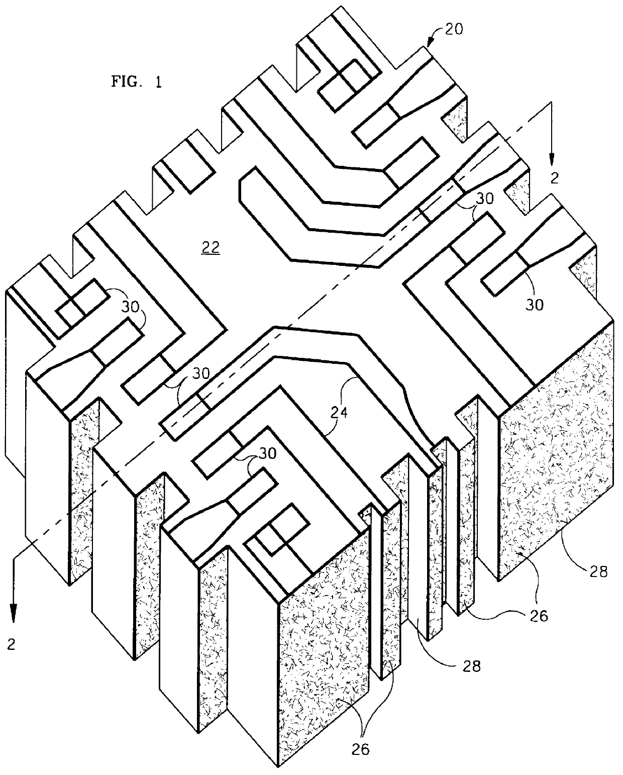
FIG. 1 is a diagrammatic perspective view showing a monolithic, buried-substrate, ceramic multiple capacitor 20 in accordance with the present invention having variable-width side castellations 28, and / or variable width conductive traces 26, as well as integral conduction traces 24 on its top surface 22. The surface 22 will be referred to for convenience as the "top" of the multiple capacitor 20, although it should be realized that the capacitor 20 has no preferred orientation. The multiple capacitor 20 can be used in any orientation, but the surface 22 is typically the last to be formed, an is often positioned on "top" during post-firing steps such as the cutting of slots, or castellations, 28, as will be explained. The surface 22 contains and displays a number of conductors, or conductive traces, 24.

The conductive traces 24 were previously printed in the surface 22 by a screening process or the like. This was typically performed after the capacitor 20 had been separated from a gre...

second embodiment

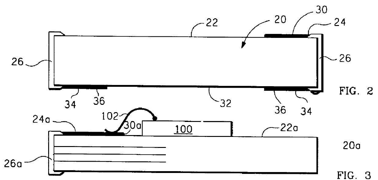
A cut-away plan view of a monolithic, buried-substrate, ceramic multiple capacitor 20a in accordance with the present invention is shown in FIG. 3. The multiple capacitor 20a mounts on its top surface an integrated circuit, or IC, 100 that is wire soldered by wire 102 (both shown in phantom line for not being a part of the present invention) to integral conduction traces 24a and pads 30a on the top surface 22a of the capacitor 20a. The integral conduction traces 24a on the top surface 22a of the capacitor 20a are themselves again connected to the plates of capacitors buried (not shown) in the multiple capacitor 20a, this time by a single metallized edge region 26a.

third embodiment

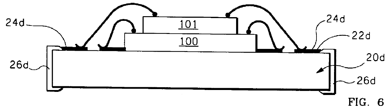
A cut-away plan view of a monolithic, buried-substrate, ceramic multiple capacitor 20b in accordance with the present invention is shown in FIG. 4. The multiple capacitor 20b mounting on its top surface an integrated circuit IC 100 that is reflow soldered to pads 30b upon the top surface 22b of the capacitor 20b over a portion of its area. and that is also wire soldered, to integral conduction traces and pads on the top surface of the capacitor. The IC 100 is also wire connected--including by ultrasonic boding or soldering--to other pads 30b upon the top surface 22b of the capacitor 20b. It may be noted that the wires 102 can connect to different ones of the pads 30b than do the reflow soldered connections, and that the wiring may be quite dense.


PUM


Abstract

Variable width electrically conductive (i) traces and (ii) pads in the forms of castellations and connecting traces upon the surfaces of volume microminiature electronic components permit variable area electrical interconnection in three dimensions, particularly of monolithic, buried-substrate, multiple ceramic capacitors to integrated circuit receivers and amplifiers to make microminiature hearing aids insertable within the ear canal. A preferred embodiment monolithic multiple capacitor with side, top and bottom surfaces has a number of electrically conductive parallel layers disposed within its body with a conductive trace extending from each layer to be exposed upon a side surface. Metallized bus strips of at least two widths extend along the side surface; relatively thinner bus strips selectively interconnecting the exposed traces to form a plurality of capacitors while the relatively thicker bus strips selectively extend at least some traces to one or more edge(s) of the top and/or bottom surfaces of the body where they may be externally connected, normally to piggy-backed components, by reflow soldering. The different-width metallized bus strips are preferably made by rectangular saw-cut slots in the body at differently spaced intervals, the rectangular saw-cuts forming castellations having a greater depth than width to reduce parasitic capacitance.

Description

All three predecessor applications are themselves divisionals of U.S. patent application Ser. Nos. 08 / 342,595 filed on Nov. 21, 1994, now abandoned for a MONOLITHIC MULTIPLE CAPACITOR to inventors Alan D. Devoe and Daniel F. Devoe, which application is a divisional of predecessor U.S. patent application 07 / 964,150 filed on Oct. 21, 1992 for a MONOLITHIC MULTIPLE CAPACITOR to inventors Alan D. Devoe and Daniel F. Devoe, a patent on which application issued on Nov. 24, 1994, as U.S. Pat. No. 5,367,430.The present application is to the same Alan D. Devoe who is a co-inventor on the three related predecessor patent applications, and the predecessor patent.The contents of all related predecessor patent applications and patents are incorporated herein by reference.1. Field of the InventionThe present invention generally concerns the provision of electrically conductive (i) traces and (ii) pads on microminiature electronic components assembled and integrated in three-dimensional, monolithi...

Claims


Application Information

Patent Timeline
Patent Type & Authority Patents(United States)
IPC IPC(8): H01L23/48H01L23/12H01L23/498H01L23/13
CPCH01L23/13H01L23/49805H01L2224/32145H01L2224/48091H01L2224/48227H01L2224/48465H01L2924/01004H01L2924/01013H01L2924/01046H01L2924/01078H01L2924/01079H01L2924/15162H01L2924/19041H01L2924/30107H01L2924/3025H01L2924/00014H01L24/48H01L2924/01019H01L2924/00H01L2224/45144H01L2224/45124H01L2924/12042H01L24/45H01L2924/14H01L2224/05599H01G4/38
Inventor DEVOE, ALAN D.DEVOE, LAMBERT T.
Owner DEVOE ALAN D
Why Eureka
Try Eureka