Multiple-function GaAs transistors with very strong negative differential resistance phenomena

a multi-function gaas transistor and negative differential resistance technology, applied in the direction of bulk negative resistance effect devices, electrical equipment, semiconductor devices, etc., can solve the problems of narrow valley current range and difficult to increase peak current valu

Inactive Publication Date: 2000-03-28
NAT SCI COUNCIL
View PDF4 Cites 14 Cited by
  • Summary
  • Abstract
  • Description
  • Claims
  • Application Information

AI Technical Summary

Problems solved by technology

In addition, since the doped efficiency of the AlGaAs is lower, attempting to increase the peak current value is not easy.
The mobility of the AlGaAs barrier is too low in the conventional real space transfer device resulting in the valley current range being narrow.

Method used


Image

  • Multiple-function GaAs transistors with very strong negative differential resistance phenomena
  • Multiple-function GaAs transistors with very strong negative differential resistance phenomena
  • Multiple-function GaAs transistors with very strong negative differential resistance phenomena

Examples


example 1

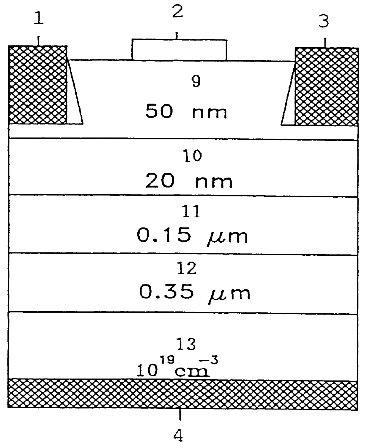
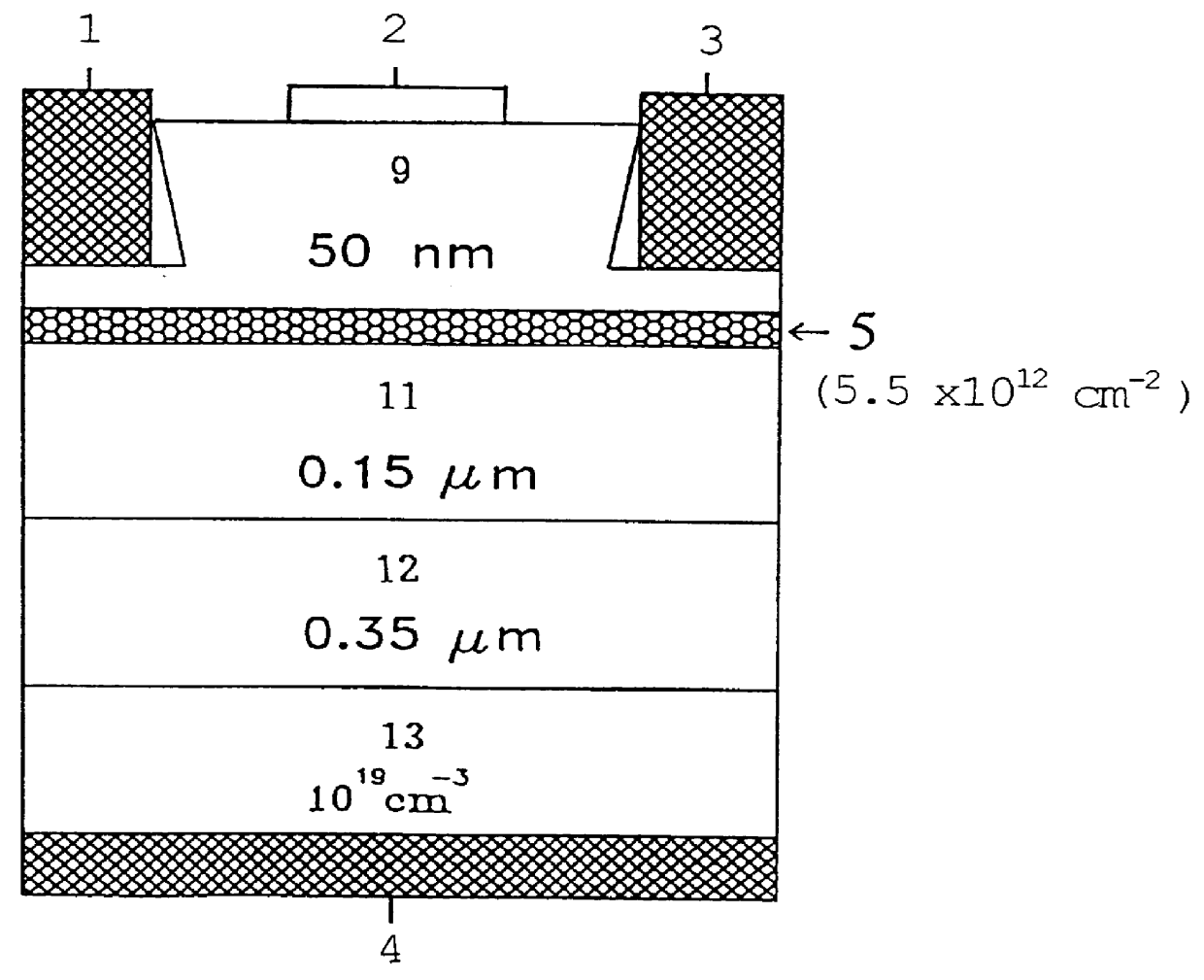
The Manufacture Process of the Devices

1. The preparation of the mesa etching

Every device should be processed through photo resistance, exposure and image development steps. The chip is dipped into the etching solution (NH.sub.4 OH:H.sub.2 O.sub.2 :H.sub.2 O=5:3:100) for 30 seconds to eliminate the photo resistance with acetone (ACE).

2. The ohmic contact metalization

The Au-Ge alloy (Au 88%, Ge 12%) is applied as the materials for the drain electrode, the source electrode and the substrate backside collector ohmic contacts. An ohmic recession is made after reprocessing the photo resistance, exposure image development, etching the cap layer with the etching solution, lifting off the photo resistance, and evaporating process. In addition, a thin silver layer is deposited on the surface of the Au--Ge alloy, and then the surface fat is eliminated through the cleaning step. Finally, the drain and source electrodes photo cap are made by using the AZ1400 positive photo resistance. The chip i...
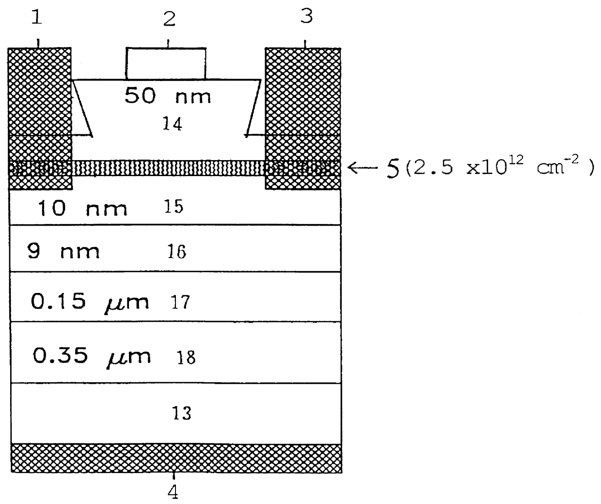
example 2

The Growth System and Epitaxy

1. The gas treating process

The hydrogen flow rate can be read from a mass flow controller. Therefore, the actual organic source flow rate can be obtained from a suitable formula.

2. The substrate cleaning step

The first basic cleaning step is dipping the substrate into various solutions and oscillating with an ultrasound device for 10 minutes. The used solutions sequentially include trichloroethylene (TCE), acetone (ACE), and methanol. Second, rinsing the substrate with an appropriate solution. The appropriate solution steps include secondary deionized water rinsing for 10 minutes, etching solution, H.sub.2 SO.sub.4 :H.sub.2 O.sub.2 :H.sub.2 O=5:1:1 for 4 to 5 minutes, rinsing for 5 minutes with secondary deionized water once again, rinsing for 1 minute with ammonia water (1:1) for eliminating the oxidation layer, and rinsing for 5 minutes with secondary deionized water once again. Third, blowing a high purity nitrogen gas then loading the substrate into a...


PUM


Abstract

Disclosed in this invention is a new four-terminal type and multiple delta-doped transistors with multiple functions grown by low-pressure metalorganic chemical vapor deposition (LP-MOCVD). All the epilayers are grown on n+-GaAs substrates. The real-space transfer transistors (RST), the collector is located under the substrate, reveal very strong negative differential resistance phenomena. The RST structure using an InGaAs channel manifests superior characteristics of a very high peak-to-valley current ratio up to 430,000 at room temperature, a peak current as high as 100 mA, very sharp charge injection, and a valley current as broad as 5.5V. Meanwhile, high performance heterostructure field effect transistors can be implemented on the same wafer by further evaporating a gate between source and drain electrodes. In order to significantly reduce leakage current, an ohmic recession is made at the source and drain. These new multiple-functions device may be used in high-speed, low-noise, and/or high power microwave oscillators and amplifiers.

Description

BACKGROUND OF THIS INVENTIONTo date, the developed S or N type negative differential resistance (NDR) devices in the world are applied extensively in the high-speed switches or high frequency oscillator. meanwhile, a real space transfer device is designed on the basis of the principle that by using voltage, electrons move at high speed to produce energy. When the energy exceeds a threshold value of the potential energy in the epitaxy, the electrons conduct (transfer) vertically to the adjacent epitaxy with the scattering effect of the atomic lattice. The change of electron location is called real space transfer (RST) . The applications of the real space transfer devices that use hot electron emission include microwave generations, high-speed logical circuits, programmable random access memory elements and photo emission devices have high potential. The major operation modes of real space transfer devices are the three terminal type negative resistance field-effect transistor (NERFET...

Claims


Application Information

Patent Timeline
Patent Type & Authority Patents(United States)
IPC IPC(8): H01L29/66H01L29/10H01L29/02H01L29/76H01L29/772
CPCH01L29/1029H01L29/1075H01L29/7606H01L29/772
Inventor HSU, WEI-CHOUWU, CHANG-LUEN
Owner NAT SCI COUNCIL
Why Eureka
Try Eureka