Use of pulsed-DC wafer bias for filling vias/trenches with metal in HDP physical vapor deposition

a technology of physical vapor deposition and pulsed dc wafer, which is applied in the direction of vacuum evaporation coating, electrolysis components, coatings, etc., can solve the problems of difficult selectively or preferentially filling trenches, vias, holes without covering field areas, and conventional sinusoidal rf bias does not accurately control the energy of ions reaching the substrate surfa

Inactive Publication Date: 2000-04-18
APPLIED MATERIALS INC
View PDF11 Cites 261 Cited by
  • Summary
  • Abstract
  • Description
  • Claims
  • Application Information

AI Technical Summary

Problems solved by technology

However, as geometries shrink it becomes more difficult to fill high aspect ratio features without forming voids in the feature.
The build up of material on the field adjacent a hole or trench leads to the problem of "shadowing" in which an overhanging edge of such material can shield or deflect sputtered material from reaching the sid

Method used


Image

  • Use of pulsed-DC wafer bias for filling vias/trenches with metal in HDP physical vapor deposition
  • Use of pulsed-DC wafer bias for filling vias/trenches with metal in HDP physical vapor deposition
  • Use of pulsed-DC wafer bias for filling vias/trenches with metal in HDP physical vapor deposition

Examples


Embodiment Construction

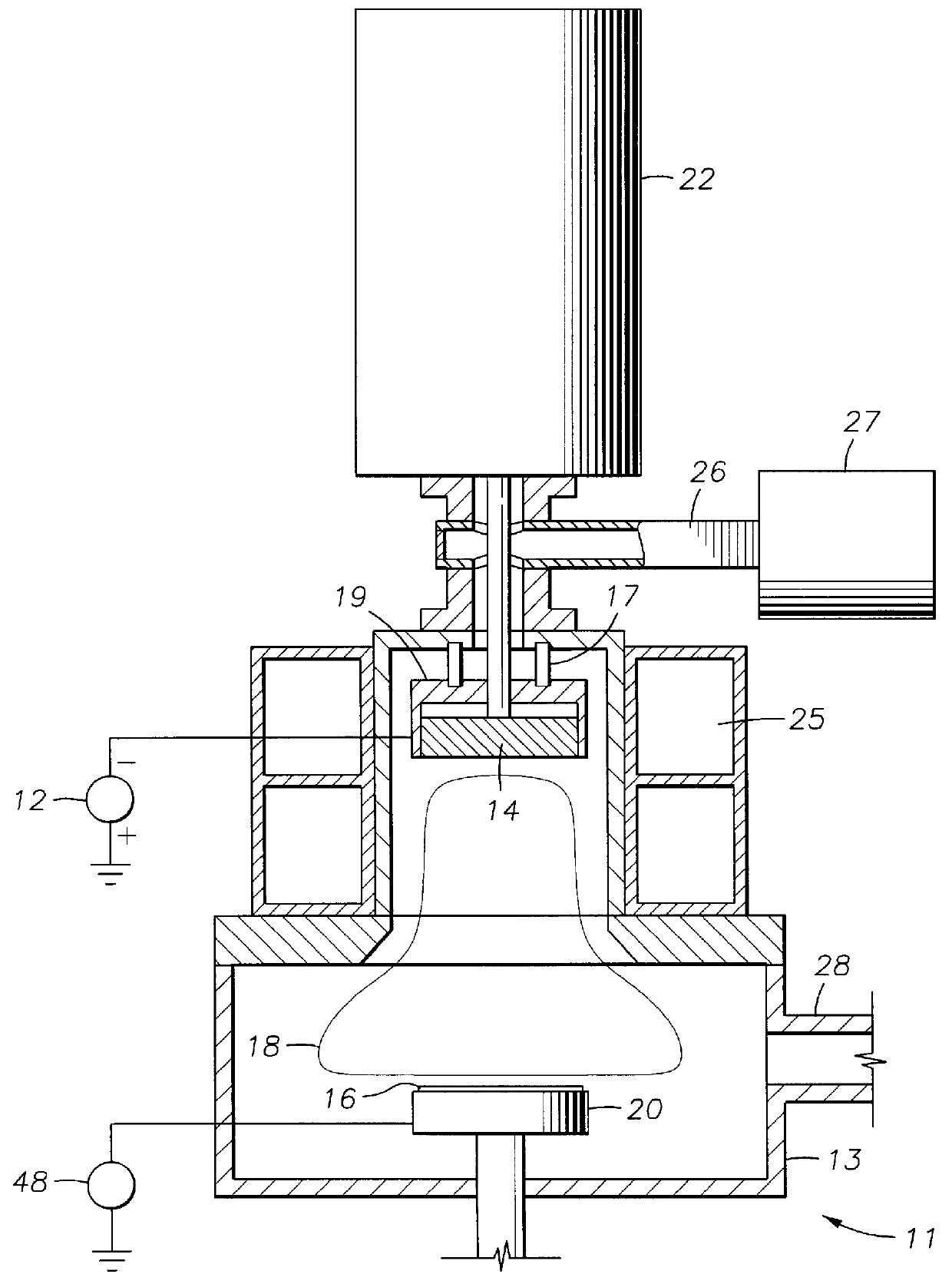
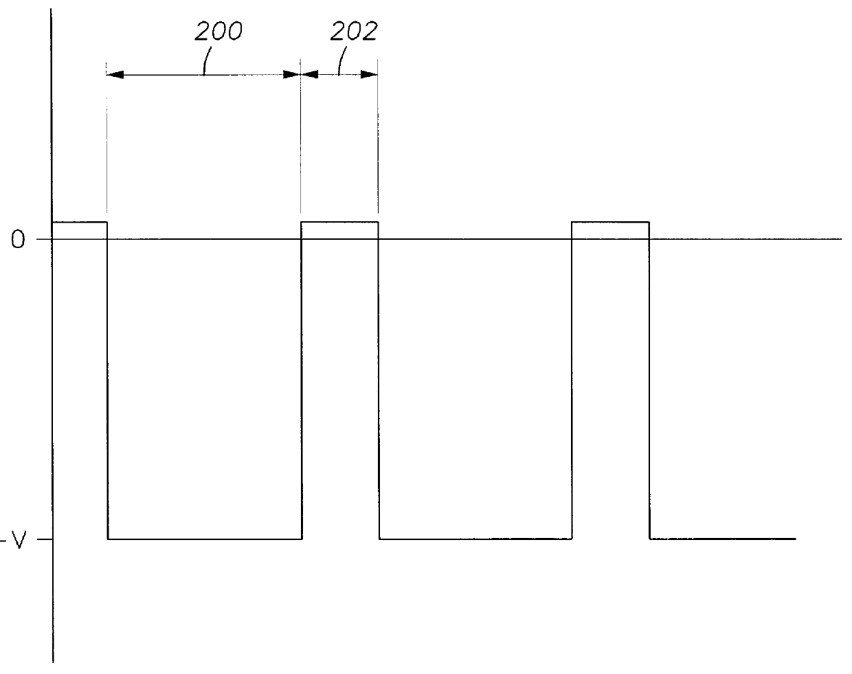
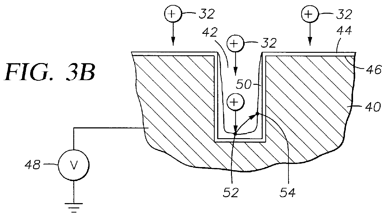
The method of the present invention was conducted on a patterned 8 inch silicon wafer plasma chamber which is substantially represented by FIG. 1. The chamber was evacuated to a base pressure of 3.times.10.sup.-7 Torr and then filled with argon to a process pressure of about 0.85 mTorr to about 1.5 mTorr. A high negative voltage of 800 V was applied to an aluminum target with a target current of 2 Amps. Upper chamber magnets were powered with 230 Amps and lower chamber magnets were powered with 180 Amps. Microwave energy was supplied to the chamber at 4 KW from an external source as described for FIG. 1. A pulsed DC bias was capacitively coupled to the substrate as shown in FIG. 1 at a maximum voltage of -40 V and a frequency of 30.5 MHz. Deposition / etching was maintained for 40 minutes and aluminum completely filled the vias / trenches in the substrate without voids.

Similar process conditions were also used with RF biasing of the substrate and with DC biasing of the substrate. RF bia...


PUM

PropertyMeasurementUnit
Fractionaaaaaaaaaa
Pressureaaaaaaaaaa
Pressureaaaaaaaaaa

Abstract

The present invention provides a method and apparatus for preferential PVD conductor fill in an integrated circuit structure. The present invention utilizes a high density plasma for sputter deposition of a conductive layer on a patterned substrate, and a pulsed DC power source capacitively coupled to the substrate to generate an ion current at the surface of the substrate. The ion current prevents sticking of the deposited material to the field areas of the patterned substrate, or etches deposited material from the field areas to eliminate crowning or cusping problems associated with deposition of a conductive material in a trench, hole or via formed on the substrate.

Description

1. Field of the InventionThe present invention relates generally to methods and apparatus for fabricating electronic devices on substrates, including integrated circuits. More particularly, the present invention relates to methods for selectively or preferentially depositing material in trenches, holes or vias formed in a substrate surface using physical vapor deposition (PVD) with a high density plasma2. Background of the Related ArtSputtering or physical vapor deposition is a known technique for depositing thin films onto a substrate. Typically in a sputtering system, a glow discharge plasma is generated in an atmosphere of inert gas by maintaining an inert gas atmosphere at a low pressure between a two electrode system comprising a cathode and an anode. A plasma is created in the space between the electrodes in which the inert gas atmosphere becomes at least partially ionized. The plasma is bounded from each of the electrodes by a plasma sheath or dark space. A high negative pote...

Claims


Application Information

Patent Timeline
IPC IPC(8): C23C14/34C23C14/35C23C14/04H01L21/70H01L21/768H01J37/32
CPCC23C14/046C23C14/34C23C14/357H01J37/32623H01L21/76877H01J37/32706H01J37/34H01L21/2855H01J37/32678C23C14/04
Inventor YAO, TSE-YONGXU, ZHENGNGAN, KENNY KING-TAICHEN, XINGURBAHN, JOHNBOURGET, LAWRENCE P.
Owner APPLIED MATERIALS INC
Why Eureka
Try Eureka