High speed crystallography detector

a crystallography and detector technology, applied in the direction of instruments, x/gamma/cosmic radiation measurement, radiofrequency control devices, etc., can solve the problems of low stopping power, poor dynamic range of films, and non-optimal sensitivity, and achieve low signal-to-noise ratio fiber optics, high signal-to-noise ratio, and avoid cumbersome effects

Inactive Publication Date: 2000-05-02
CONTINENTAL AUTONOMOUS MOBILITY US LLC
View PDF4 Cites 19 Cited by
  • Summary
  • Abstract
  • Description
  • Claims
  • Application Information

AI Technical Summary

Benefits of technology

The invention further comprises large sized area sensors, having two or three dimensional arrays of high signal-to-noise ratio hybrid chips where each hybrid is composed of a detector array and readout unit cell array chip. These hybrid arrays avoid cumbersome, low signal-to-noise ratio fiber optics, slow CCD readout arrays and lower than room temperature operatio

Problems solved by technology

Film has poor dynamic range and non-optimal sensitivity because of low stopping power, particularly for higher crystallographic x-ray energies.
However, in spite of the greater SP stopping power, SP sensitivity is relatively as low as film because of photon losses in the readout system See E. F. Eikenberry, et al, "X-ray Detectors: Comparison of Film, Storage Phosphors and CCD detectors", Conference on Photoelectronic Image Devices, London, September, 1991, Section 3.
Because of either their low stopping power or low x-ray quantum efficiency and long readout time, film and SP imaging plates perform poorly as synchrotron radiation detectors.
Charge Coupled Device (CCD)-based detectors are superior to film and storage phosphor imaging plates in performance and convenience; however, they are limited by low signal-to-noise ratio, poor read out efficiency, limited effective temperatures of operation and poor time resolution compared to the present invention.
Higher resolution requirements also lead to larger detector area requirements.
Loss of more than 95% of the visible photons in making a direct transition from the phosphor to the CCD is common, resulting in low gain and, consequently, in a single-x-ray-photon signal which is well below the sensor noise and cannot be detected.
A weak link in low-signal detector designs is the image intensifier which, because of the low quantum efficiency of its photocathode or its large noise factor, results in a less than optimal DQE (about 50%-75%) and also causes inconvenient image distortion.
But the waiting times are excessive and preclude effective real time use.
In addition, faint diffraction patterns may be undetected.
The CCD itself creates inherent time-resolution problems with the CCD-based detector designs resulting in considerable dead time when no l

Method used


Image

  • High speed crystallography detector
  • High speed crystallography detector
  • High speed crystallography detector

Examples


Embodiment Construction

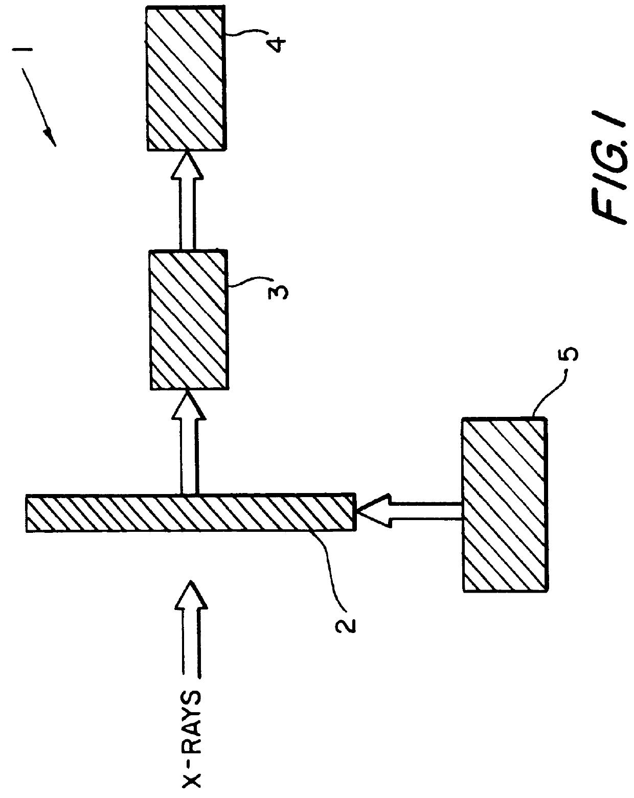
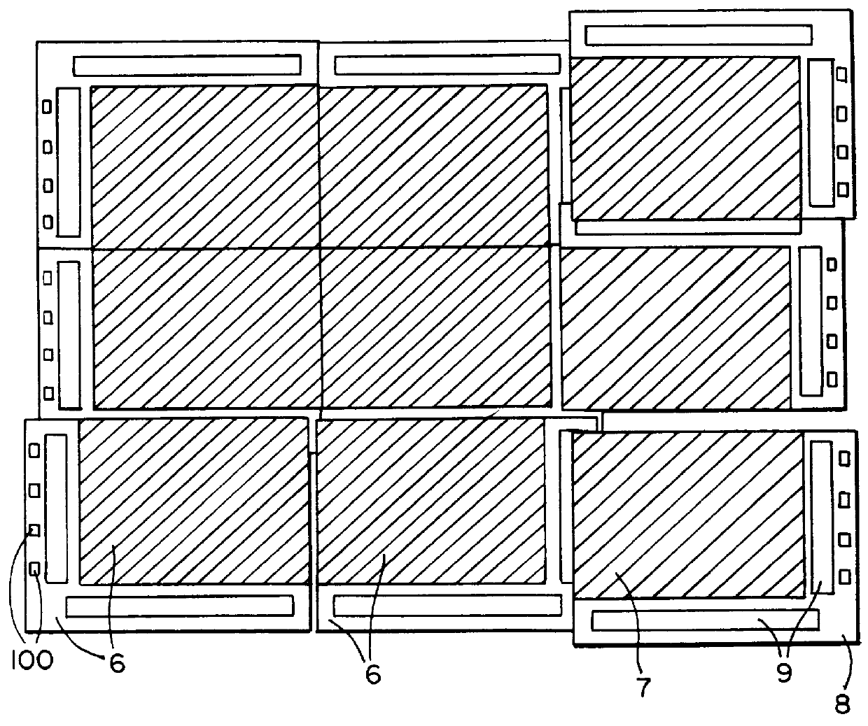
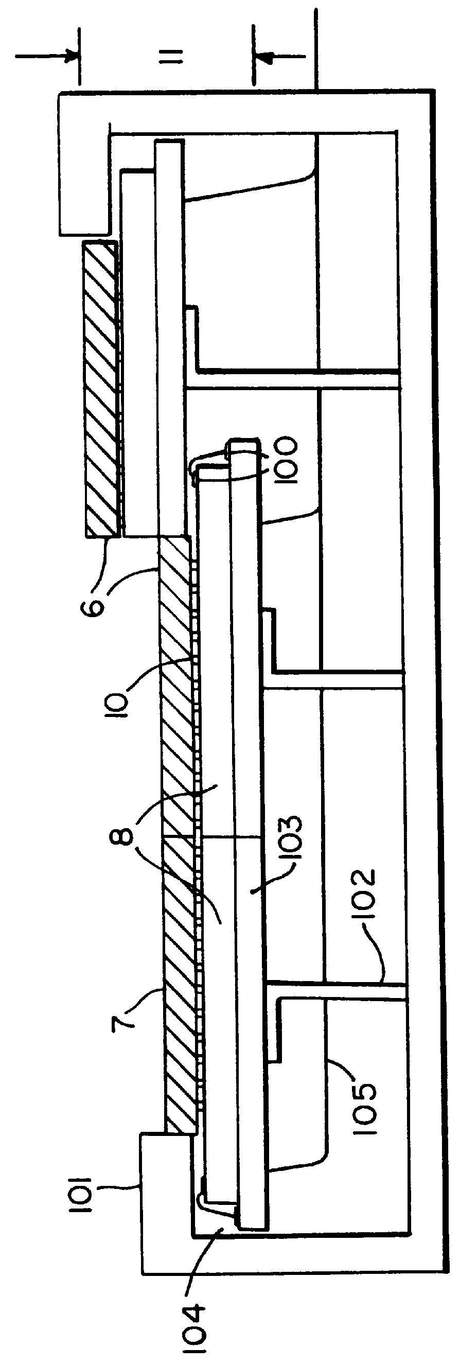
A preferred embodiment of the present invention is a high Detective Quantum Efficiency (DQE), high-speed, solid-state device, designed to sense and digitize diffraction data obtained by the passage of x-rays through a crystal. FIG. 1 is a block diagram of an embodiment of the invention, which is termed a High-Speed Crystallography Detector (HSCD) system 1. This system 1 is comprised of an area sensor 2, digitizing and output electronics 3, a data processor 4 and area-sensor drive electronics 5. FIG. 2A, a top view, and FIG. 2B, a side view, show in further detail the area sensor 2 of a preferred embodiment of the present invention. The area sensor 2 is comprised of multiple hybrids 6, comprised of detector array chips 7 hybridized to readout array chips 8 and arranged in a two or three dimensional configuration. Electrical connections are made to the readout array chip 8 by means of wire bond pads 100. The support structure is detailed in FIG. 2B and consists of a metal frame 101, c...


PUM


Abstract

A device for the collection, digitization and analysis of synchrotron x-ray crystallographic data using an area detector which detects x-ray photons directly on arrays of solid state detectors and stores the information on capacitors located on readout unit cell array chips. The device consists of a two dimensional area detector, for amplification, collection and conversion of the diffracted x-rays to electrical signals, drive electronics for providing the timing pulses and biases to the area sensor, output electronics for converting the x-ray signals to digital signals and storing the signals, and a data processor to analyze the digital signal form the output electronics. The solid-state detector array is made up of a variable-area three-dimensional array of detector array chips where each chip is in turn made up of an array of solid-state detectors. Each detector on the detector array chip is electrically connected to a readout unit cell on a readout array chip directly beneath the detector array chip. The readout unit cell contains the circuitry for storage, switching and readout of the x-ray signals.

Description

This invention relates to electronic apparatus for capturing and digitizing x-ray patterns. More particularly, it relates to apparatus for imaging the x-ray pattern resulting from the diffraction of x-rays by crystals.X-ray diffraction patterns are useful in the analysis of molecular structures, such as protein and virus molecules. Protein and virus crystallography imposes stringent requirements on x-ray detectors, particularly where the x-ray source is high flux synchrotron radiation that enables an experiment to be done rapidly. Furthermore, an important and developing protein-crystallography field is time-resolved crystallography using synchrotrons. Monitoring a time-dependent reaction in a crystal can elucidate the time-dependent molecular changes that occur in a chemical reaction. High time resolution speed is often critical to such monitoringFilm has traditionally been used in crystallographic analysis but now competes with storage phosphor (SP) imaging plates. Film has poor d...

Claims


Application Information

Patent Timeline
IPC IPC(8): G01T1/20G01T1/00G01T1/29G01T1/24
CPCG01T1/2018G01T1/247G01T1/2928G01T1/2006
Inventor STETTNER, ROGERBAILEY, HOWARD
Owner CONTINENTAL AUTONOMOUS MOBILITY US LLC
Why Eureka
Try Eureka