Silicon single crystal wafer having few defects wherein nitrogen is doped and a method for producing it
a single crystal wafer and silicon single crystal technology, which is applied in the direction of silicon compounds, silicon single crystal growth, silicates, etc., can solve the problems of reducing the efficiency of the furnace of the growing crystal apparatus (hot zone: hz), difficult to expand the n-region to an axial direction of crystal growth, and defects in fz silicon in a silicon single crystal
- Summary
- Abstract
- Description
- Claims
- Application Information
AI Technical Summary
Benefits of technology
Problems solved by technology
Method used
Image


Examples
example 1
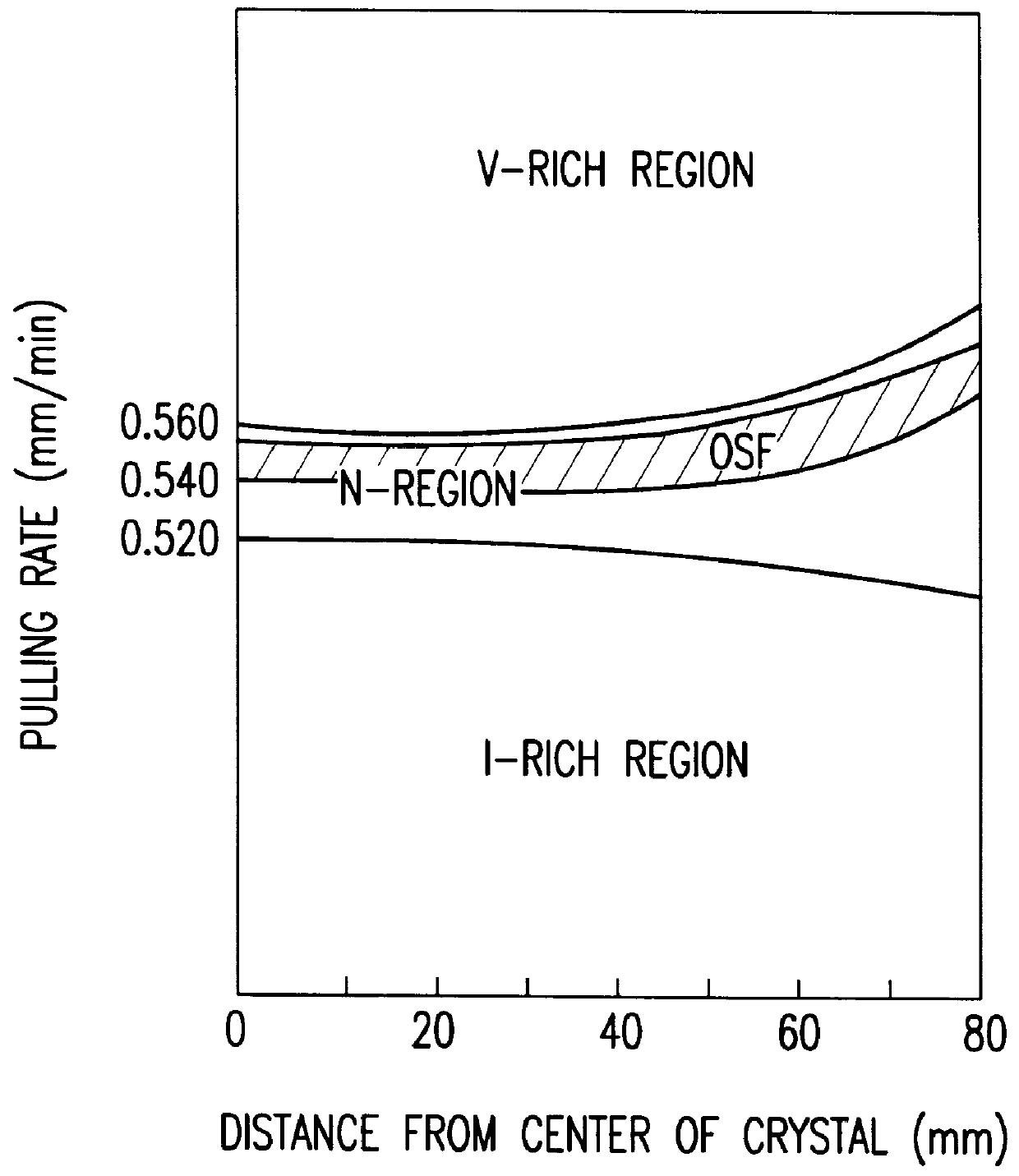
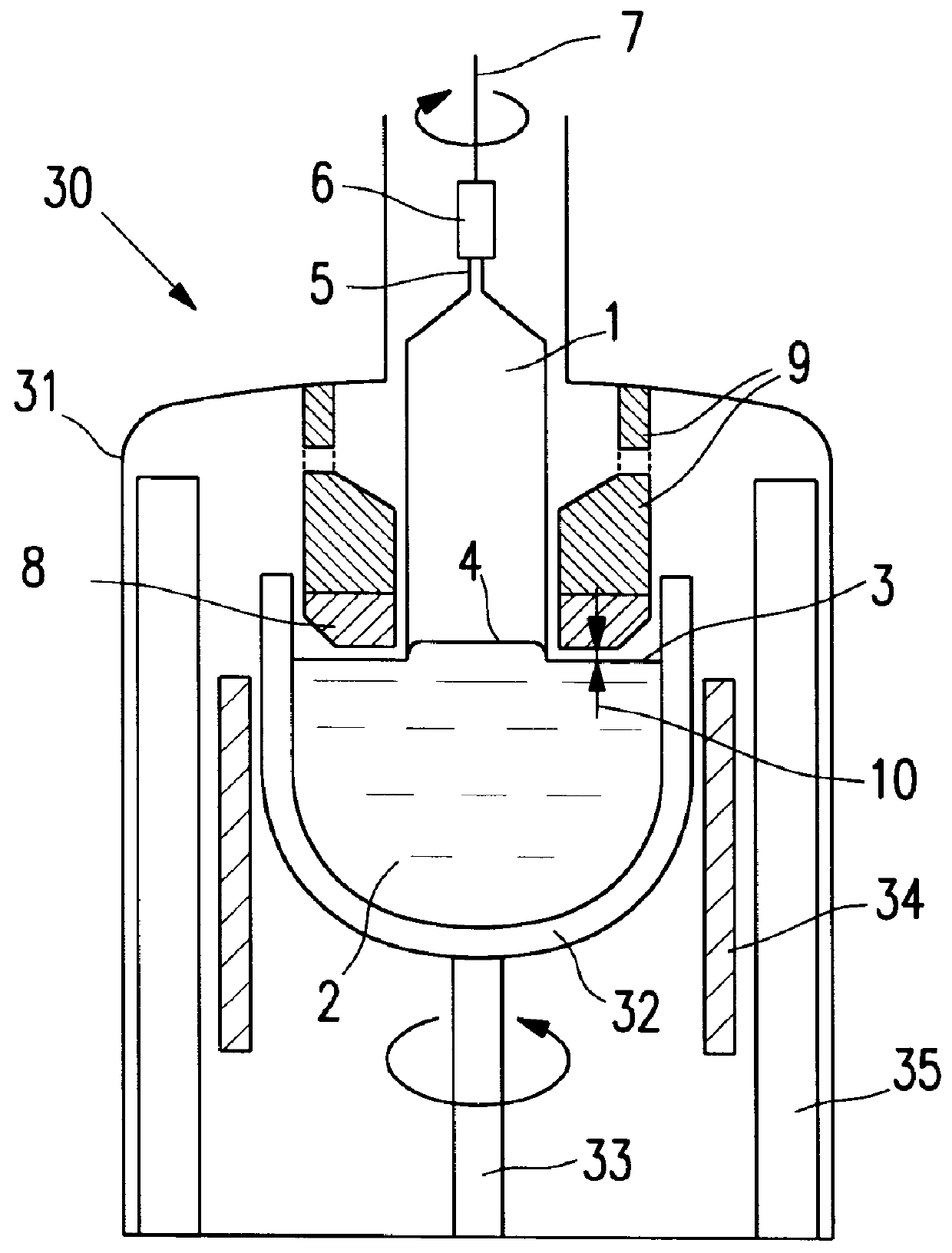
A silicon single crystal was grown through use of the crystal pulling apparatus 30 of FIG. 3. Polycrystalline material of silicon was charged into a quartz crucible having a diameter of 18 inches. A single crystal ingot of p-type having a diameter of 6 inches and orientation was pulled at a magnetic field intensity of 3000 G, at a number of rotation of a crucible of 4 rpm and at a number of rotation of crystal of 15 rpm with varying a pulling rate over the range of 0.57 to 0.50 mm / min.
The temperature of a silicon melt was 1420.degree. C. An annular solid-liquid interface insulator having a height of 10 cm was disposed above the melt surface such that a gap of 4 cm was formed between the melt surface and the bottom end of the interface insulator. Through adjustment of a crucible-holding shaft, the height of a ceiling of a pull chamber was adjusted to 30 cm above the melt surface. An upper surrounding insulator was disposed on the interface insulator.
A doping amount of nitrogen was 1...
example 2
The silicon single crystal ingot was pulled in the same method as Example 1 except that oxygen concentration was 14 ppma (JEIDA). Wafers were sliced from the thus obtained single crystal ingot, and subjected to a heat treatment of 800.degree. C..times.4 hours+1000.degree. C..times.16 hours. A density of defects in the wafer after the heat treatment was measured.
The defect density was measured with OPP (Optical Precipitate Profiler manufactured by Bio-Rad).
The result was 5.times.10.sup.9 to 7.times.10.sup.10 number / cm.sup.3, which was higher than a conventional silicon wafer, and shows higher gettering effect of the wafer.
PUM
 Abstract
Description
Claims
Application Information