Method for producing semiconductor device

a technology of semiconductors and semiconductor films, applied in the direction of semiconductor devices, basic electric elements, electrical appliances, etc., can solve the problems of increasing manufacturing costs, difficult to form uniform filmes having excellent semiconductor physical properties on the whole surface of substrates, and inferior physical properties of silicon semiconductors such as electrical conductivity,

Inactive Publication Date: 2000-09-19
SEMICON ENERGY LAB CO LTD
View PDF43 Cites 40 Cited by
  • Summary
  • Abstract
  • Description
  • Claims
  • Application Information

AI Technical Summary

Problems solved by technology

However, this type of silicon semiconductor has inferior physical properties such as electrical conductivity, etc. to the crystalline silicon semiconductor.
However, in the method (1), it is technically difficult to form a film having excellent semiconductor physical properties on the whole surface of a substrate uniformly.
In addition, the film formation must be performed at a temperature above 600.degree. C. and thus an inexpensive glass substrate is unusable, so that a manufacturing cost is increased.
In this case, the irradiation area of the laser beam is small, and thus this method has a disadvantage that a throughput is low.
In addition, the stability of the laser beam is insufficient, so that the whole surface of a large-area substrate cannot be treated uniformly.
That is, this method is not practically usable at present.
However, this method requires a heating temperature above 600.degree. C., and thus an inexpensive glass substrate is not usable.
When a large-size glass substrate is used, contraction and distortion of a substrate occur in a heating process which is indispensable to produce semiconductors, and they cause a critical problem that the precision of a masking process is reduced

Method used


Image

  • Method for producing semiconductor device
  • Method for producing semiconductor device
  • Method for producing semiconductor device

Examples


embodiment 1

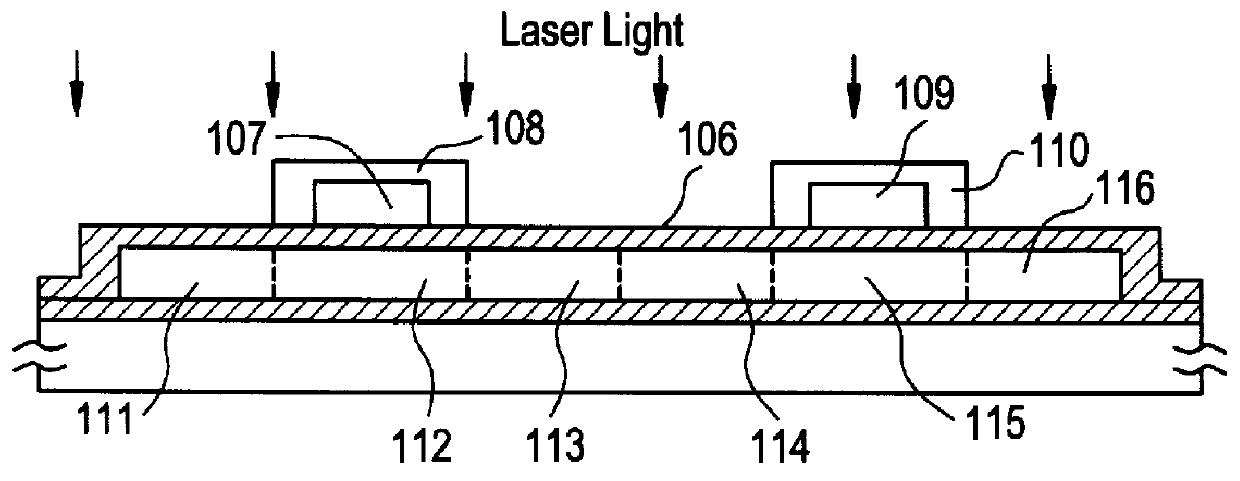
Then, the silicon layer 603 is etched to form TFT regions. A silicon oxide layer 609 is formed on the entire surface to a thickness of 1000-1500 .ANG., for example, 1200 .ANG.. Also, in the same manner , a gate electrode 610 for a PTFT and a gate electrode 613 for an NTFT made of aluminum, an anoxic oxidation film 612, 614 are formed to obtain a gate portion of the TFT.

first embodiment

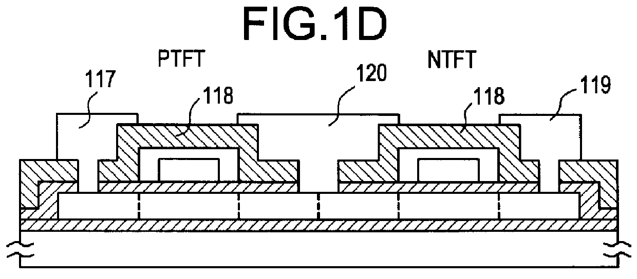
Then, an n-type impurity and a p-type impurity are respectively introduced into the semiconductor layer by using the gate portion as a mask. As a result, source 615, channel 616, drain 617 of the PTFT and source 620, channel 619 and a drain 618 of the NTF for a peripheral circuit are formed. Subsequently, a laser irradiation is performed on the entire surface of the structure in order to activate the doped impurity in the same manner as in the (FIG. 6D)

Finally, a silicon oxide layer 621 is formed to a thickness of 3000-8000 .ANG., for example, 5000 .ANG. as an interlayer insulating film, following which contact holes are opened for source and drain regions of the TFTs, and a double-layer of titanium nitride (1000 .ANG. thick) and aluminum (5000 .ANG.) are deposited by sputtering to form electrode / wirings 622-644. In the manner described above, an inventor circuit of a PTFT and an NTFT comprising a crystalline silicon in which the crystal growth occurred in a lateral direction. (FIG...


PUM


Abstract

A silicon film provided on a blocking film 102 on a substrate 101 is made amorphous by doping Si+, and in a heat-annealing process, crystallization is started in parallel to a substrate from an area 100 where nickel serving as a crystallization-promoting catalyst is introduced.

Description

1. Field of the InventionThis invention relates to a semiconductor device having TFTs (thin film transistors) provided on an insulating substrate of glass or the like, and a method for producing the semiconductor device.2. Description of Related ArtTFTs have been conventionally formed on a glass substrate to form a semiconductor device such as an active matrix liquid crystal device or an image sensor. The TFTs are used, for example, to drive the pixels of the liquid crystal device.The TFTs used in the above devices are generally formed of a silicon semiconductor layer in the form of a thin film. The silicon semiconductor of a thin-film type is classified into two types, an amorphous silicon semiconductor (a-Si) type and a crystalline silicon semiconductor type. The amorphous silicon semiconductor can be relatively easily produced at a low film-forming temperature by a vapor-phase deposition method. Therefore, this type is suitable for mass production, and it has been most generally ...

Claims


Application Information

Patent Timeline
IPC IPC(8): H01L21/02H01L21/70H01L21/20H01L21/336H01L21/84H01L27/12H01L21/77H01L29/04
CPCH01L21/2022H01L21/2026H01L27/12H01L29/04H01L29/66757H01L27/1277H01L21/02686H01L21/02488H01L21/02491H01L21/02422H01L21/02502H01L21/02496H01L21/02532H01L21/02672H01L21/02694
Inventor ZHANG, HONGYONGTAKAYAMA, TORUTAKEMURA, YASUHIKO
Owner SEMICON ENERGY LAB CO LTD
Why Eureka
Try Eureka