
Method for producing a semiconductor device including doping with a catalyst that is a group IV element

a technology of semiconductor devices and catalysts, applied in semiconductor devices, radio frequency controlled devices, electrical apparatus, etc., can solve the problems of reducing the precision of masking process, and affecting the appearance of the masking process

Inactive Publication Date: 2000-12-12
SEMICON ENERGY LAB CO LTD
View PDF41 Cites 59 Cited by
  • Summary
  • Abstract
  • Description
  • Claims
  • Application Information

AI Technical Summary

Benefits of technology

The crystallization mechanism can be considered to be classified into two stages which are an initial nucleus generation stage and a subsequent crystal growth stage from the nuclei. The speed of the initial nucleus generation can be detected by measuring measuring a time elapsing until spotted fine crystals occur at a constant temperature. This time could be shortened in all cases where the thin films of the above kinds of impurity metal were formed on the substrate, and the effect of the introduction of the crystal nuclei on the lowering of the crystallization temperature can be proved. As an unexpected result, through an experiment for examining variation of growth of crystal grains with variation of the heating time after generation of crystal nuclei, it was observed that the speed of the crystal growth after the generation of the nuclei was also rapidly increased when a thin film of a certain kind of metal was formed on a substrate, an amorphous silicon thin film was formed on the metal thin film and then the amorphous silicon thin film was crystallized. A mechanism for this effect has not yet been elucidated at present, however, it is guessed that any catalytic effect acts.
As is apparent from the foregoing, formation of an amorphous silicon thin film after a trace lead thin film is formed enables the lowering of the crystallization temperature and the shortening of the crystallization time. This process will be described in more detail on the assumption that this process is applied to a TFT producing process. As described later, the same effect can be obtained by forming a lead thin film on not only a substrate, but also on an amorphous silicon thin film, or by implanting the lead into the amorphous silicon by an ion implantation method. Accordingly, these treatments are commonly referred to as "trace lead addition" in the specification of this application.
It has been known that the trace lead addition can provide the same effect on the lowering of the crystallization temperature in both cases where a trace lead thin film is formed on a substrate and then an amorphous silicon thin film is formed on the trace lead thin film, and where an amorphous silicon film is formed and then a trace lead thin film is formed on the amorphous silicon film, and any film-forming method such as a sputtering method, a deposition method, spin coating, coating or the like may be used as a film-forming method. However, in the method of forming the trace lead thin film on the substrate, the effect becomes more remarkable by forming a silicon oxide film on a 7059 glass substrate and then forming the trace lead thin film on the silicon oxide film than by directly forming the trace lead thin film on the substrate. As one of reasons for this fact, it would be considered that direct contact between silicon and lead is important for the low-temperature crystallization, and components other than silicon serves to obstruct direct contact or reaction between silicon and lead in the case of using a 7059 glass substrate.

Problems solved by technology

However, this type of silicon semiconductor has inferior physical properties such as electrical conductivity, etc. to the crystalline silicon semiconductor.
However, this method requires a heating temperature above 600.degree. C., and thus an inexpensive glass substrate is not usable.
When a large-size glass substrate is used, contraction and distortion of a substrate occur in the heating process which is indispensable to produce crystalline semiconductors, and they cause a critical problem that the precision of a masking process is reduced.
In addition to the heat problem as described above, a heating time required for crystallization is over several tens hours in a present process, and thus the heating time must be shortened.
A mechanism for this effect has not yet been elucidated at present, however, it is guessed that any catalytic effect acts.
However, through more delicate observation of the laterally-growing area of the crystals on the transmission electron microscopic photograph, areas containing crystals growing in a branch form was also observed upon viewing from the upper side of the substrate although the crystallization direction of needle or pillar crystals was parallel to the surface of the substrate.
Crystal components of a substrate material existing in a substrate or at an interface portion between the substrate and a semiconductor film, or crystal components in the semiconductor film can serve as nuclei for crystal growth, however, these components obstruct the crystal growth in an uniform direction (unidirection) and promote a random crystal growth in the lateral crystal growth process.
If the crystallization temperature is too high, a problem in heat resistance of the glass substrate occurs like the prior art.

Method used


Image

  • Method for producing a semiconductor device including doping with a catalyst that is a group IV element
  • Method for producing a semiconductor device including doping with a catalyst that is a group IV element
  • Method for producing a semiconductor device including doping with a catalyst that is a group IV element

Examples


embodiment 1

Then, the silicon layer 603 is etched to form TFT regions. A silicon oxide layer 609 is formed on the entire surface to a thickness of 1000-1500 .ANG., for example, 1200 .ANG.. Also, in the same manner , a gate electrode 610 for a PTFT and a gate electrode 613 for an NTFT made of aluminum, an anoxic oxidation film 612, 614 are formed to obtain a gate portion of the TFT.

first embodiment

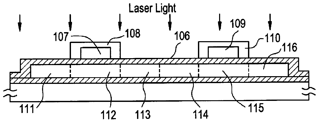
Then, an n-type impurity and a p-type impurity are respectively introduced into the semiconductor layer by using the gate portion as a mask. As a result, source 615, channel 616, drain 617 of the PTFT and source 620, channel 619 and a drain 618 of the NTF for a peripheral circuit are formed. Subsequently, a laser irradiation is performed on the entire surface of the structure in order to activate the doped impurity in the same manner as in the (FIG. 6D).

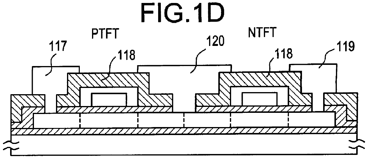
Finally, a silicon oxide layer 621 is formed to a thickness of 3000-8000 .ANG., for example, 5000 .ANG. as an interlayer insulating film, following which contact holes are opened for source and drain regions of the TFTs, and a double-layer of titanium nitride (1000 .ANG. thick) and aluminum (5000 .ANG.) are deposited by sputtering to form electrode / wirings 622-644. In the manner described above, an invertor circuit of a PTFT and an NTFT comprising a crystalline silicon in which the crystal growth occurred in a lateral direction. (FI...


PUM


Abstract

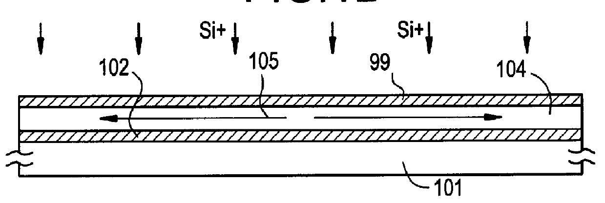
A silicon film provided on a blocking film 102 on a substrate 101 is made amorphous by doping Si+, and in a heat-annealing process, crystallization is started in parallel to a substrate from an an 100 where lead serving as a crystallization-promoting catalyst is introduced.

Description

1. Field of the InventionThis invention relates to a semiconductor device having TFTs (thin film transistors) provided on an insulating substrate of glass or the like, and a method for producing the semiconductor device.2. Description of Related ArtTFTs have been conventionally formed on a glass substrate to form a semiconductor device such as an active matrix liquid crystal device or an image sensor. The TFTs are used, for example, to drive the pixels of the liquid crystal device.The TFTs used in the above devices are generally formed of a silicon semiconductor layer in the form of a thin film. The silicon semiconductor of a thin-film type is classified into two types, an amorphous silicon semiconductor (a-Si) type and a crystalline silicon semiconductor type. The amorphous silicon semiconductor can be relatively easily produced at a low film-forming temperature by a vapor-phase deposition method. Therefore, this type is suitable for mass production, and it has been most generally ...

Claims


Application Information

Patent Timeline
IPC IPC(8): H01L21/02H01L21/20
CPCH01L21/2022H01L21/02667H01L21/02686H01L21/02502H01L21/02422H01L21/02488H01L21/02491H01L21/02532H01L21/02496H01L21/02595H01L21/02675H01L21/02672
Inventor ZHANG, HONGYONGTAKAYAMA, TORU
Owner SEMICON ENERGY LAB CO LTD
Learn More