Structure for thin film interconnect

a thin film interconnection and structure technology, applied in the direction of electrical equipment, metal layered products, solid-state devices, etc., can solve the problems of high production cost, inability to meet the requirements of the finished product, and the previous built layer is exposed to the entire process excursion, so as to achieve the effect of providing dimensional stability to the structur

Inactive Publication Date: 2000-12-26
IBM CORP
View PDF13 Cites 31 Cited by
  • Summary
  • Abstract
  • Description
  • Claims
  • Application Information

AI Technical Summary

Benefits of technology

One object of this invention is to provide a method for fabrication of a compensator for use in multilayer thin film structures to serve as a ground / reference plane for the signal wiring, and to provide dimensional stability to the structure.

Problems solved by technology

The approach based on sequential building of each layer to form high-density wiring structures, however, suffers from the problem that every time a new layer is fabricated, the previously built layers are exposed to the entire process excursions including thermal, chemical / solvents, mechanical and other stress-related operations.
In addition, since the electrical performance and long-term reliability of the sequentially built structure can only be determined after the conclusion of the entire fabrication process, the finished part may have to be discarded if the performance does not meet the required specifications.
This results in high cost of production, and has other obvious limitations in terms of cycle time / throughput.
This is due to the fact that the thin polymer films, such as polyimide films, are generally fragile and flexible, and are subject to deformation under thermal or solvent-related stress conditions.
This can result in pattern misalignment / distortion during layer fabrication or in the process of lamination and also when the composite structure undergoes accelerated reliability tests involving temperature and humidity excursions.
However, the process according to this process would suffer the limitations of potential pattern misalignment / distortion mentioned above.

Method used


Image

  • Structure for thin film interconnect
  • Structure for thin film interconnect
  • Structure for thin film interconnect

Examples


Embodiment Construction

The following example is intended to further illustrate the invention and is not intended to limit the scope of the invention in any manner.

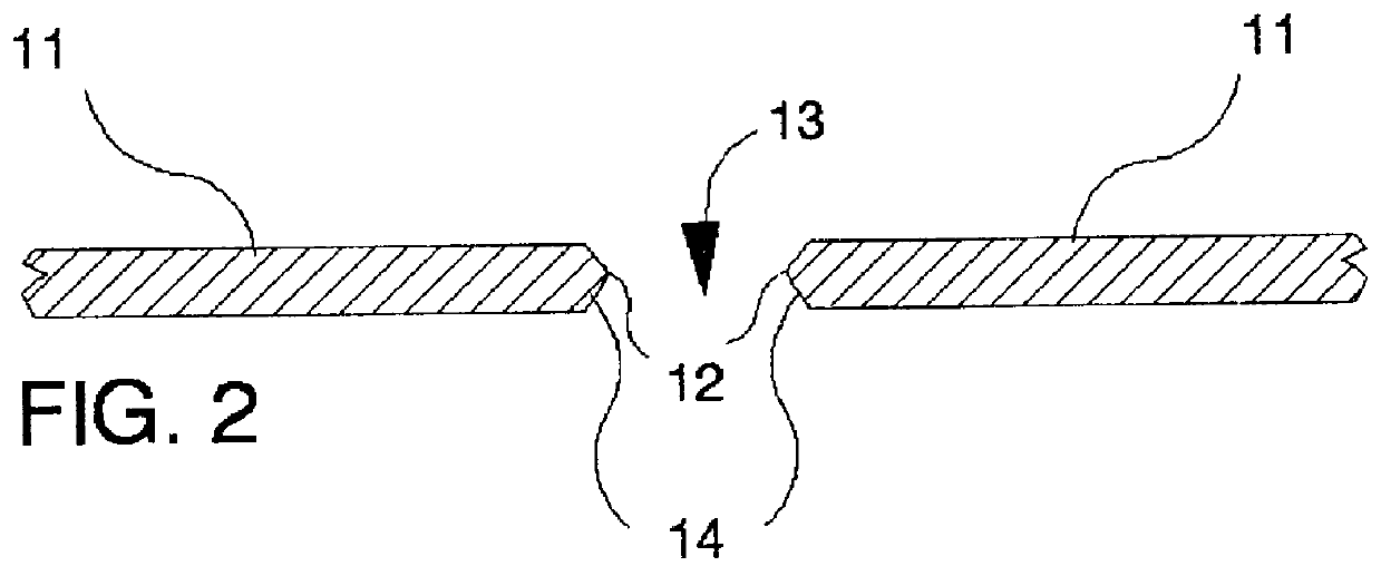
Double-sided etched molybdenum (1.4 mil thick) with knife-edge vias is made according to molybdenum etch techniques using photoresists and masks which are well known in the art. See for example, "Screening Masks and Method of Fabrication" I.B.M. Technical Disclosure Bulletin, Vol. 20, No. 2, pp. 577-578, (July 1977).

A thin layer (200-500A) of chromium is evaporated onto both sides of the etched molybdenum foil such that it not only forms a continuous film on the top and bottom surfaces, but also forms a conformal film on the via sidewalls.

For use as a rigid support, a glass plate is coated on one side with 10 micron of polyimide which is fully cured. This polymer application is accomplished by means of spin, spray, or roller coating. A layer of chromium-copper-chromium metallurgy is then sputtered on top of this initial layer of polymer. The top...


PUM

PropertyMeasurementUnit
thickaaaaaaaaaa
pressureaaaaaaaaaa
thickaaaaaaaaaa

Abstract

This invention relates generally to a structure and process for thin film interconnect, and more particularly to a structure and process for a multilayer thin film interconnect structure with improved dimensional stability and electrical performance. The invention further relates to a process of fabrication of the multilayer thin film structures. The individual thin film structure is termed a compensator, and functions as both a ground/reference plane and as a stabilizing entity with regard to dimensional integrity. The compensator is comprised primarily of a metal sheet having a metallized via pattern and high-temperature stable polymer as an insulator.

Description

This invention relates generally to a structure and process for a thin film interconnect, and more particularly to a structure and process for multilayer thin film interconnect structures with improved dimensional stability and electrical performance. The invention further relates to a process of fabrication of the particular multilayer thin film structure, termed a "compensator", which functions as a ground plane (i.e., a reference plane). The compensator is comprised primarily of a metal sheet having a metallized via pattern and a high-temperature stable polymer as an insulator.Fabrication of multilayer thin film interconnect structures for high-density integrated circuits generally involves sequential build of metal-patterned dielectric layers on silicon or ceramic substrates. Among the various dielectric / insulator materials which are generally used in the thin film structures, are sputtered or Plasma Enhanced Chemical Vapor Deposition (PECVD) quartz, silicon nitride, and high-te...

Claims


Application Information

Patent Timeline
Patent Type & Authority Patents(United States)
IPC IPC(8): H01L21/48H01L21/02H01L23/538H01L23/52H05K3/46H05K3/44H05K3/00H05K3/42H05K3/38H05K3/40H01L23/522C08G73/10H01L21/768H05K1/05
CPCH01L21/486H01L23/5384H05K3/445H05K3/4641H01L23/5383Y10T428/12556H05K3/0032H05K3/0035H05K3/0061H05K3/007H05K3/388H05K3/4076H05K3/423H05K3/4614H05K3/4617H05K2201/0154H05K2201/068H05K2201/09554H05K2201/09563H05K2201/096H05K2203/0152H01L2924/0002Y10T428/12806Y10T428/12361Y10T29/49165Y10T428/24777Y10T428/12382Y10T428/12812Y10T428/12569H01L2924/00Y10T428/31678Y10T428/31681
Inventor SACHDEV, KRISHNA GANDHIKELLNER, BENEDIKT MARIA JOHANNESMCGUIRE, KATHLEEN MARYSORCE, PETER JEROME
Owner IBM CORP
Why Eureka
Try Eureka