Electrical detector for micro-analysis systems

Inactive Publication Date: 2001-01-02
UTAH RES FOUND UNIV OF THE
View PDF16 Cites 241 Cited by
  • Summary
  • Abstract
  • Description
  • Claims
  • Application Information

AI Technical Summary

Benefits of technology

The detection system of the present invention provides many benefits and advantages over prior detectors. Some of the advantages of the detector include simplicity of design and operation, fast response and short warm-up time, high signal-to-noise ratio, detection of a wide range of sample types, small size, and compatibility with micromachining processes and very large scale integration (VLSI) technology for signal processing. The detector can be employed in a wide range of applications and allows detection of a wide range of analytes.
In particular, the detection system of the invention provides for high resolution measurement of the electrical characteristics of biological systems, as wells as other small samples of materials in liquids or gases as small as 1 femtoliter, which have been separated by a biological or chemical micro-analysis system. By incorporating the detector onto the same chip as the micro-analysis system, the detector can achieve a higher degree of resolution than conventional off-chip detectors. The detector can monitor the presence and the concentration of various t

Problems solved by technology

In the case of living organisms, pipette based methods suffer the disadvantage of being inherently invasive and require access to the intracellular space.
This presents a problem in that a priori models describing the shape of the cell and the constitutive properties within the cell are required to estimate the dielectric parameters.
Although this micro-ER device is capable of somewhat smaller spatial resolution, the device still suffers from the aforementioned difficulties generally associated with ER systems, and in addition, fails to resolve electrical characteristics on a subcellular level.
Although the Lo system is usefull in providing additional information on the resistive and capacititve properties of cells and cell membranes, the system fails to resolve electrical characteristics on a subcellular level.
They are generally very bulky, expensive, complex, and often require modificat

Method used


Image

  • Electrical detector for micro-analysis systems
  • Electrical detector for micro-analysis systems
  • Electrical detector for micro-analysis systems

Examples


Example

EXAMPLE 2

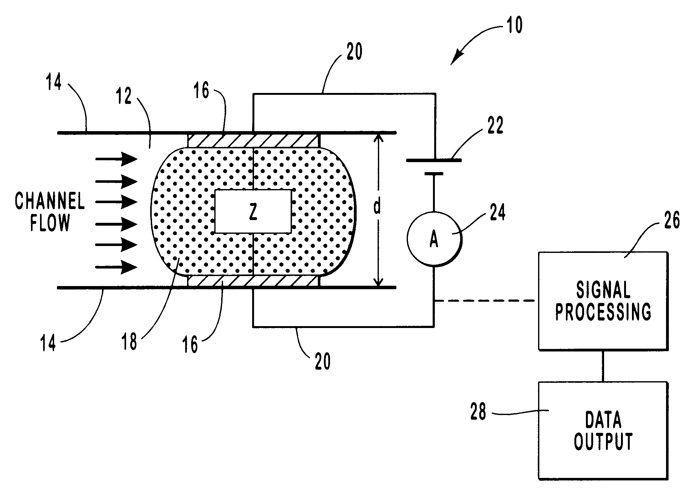
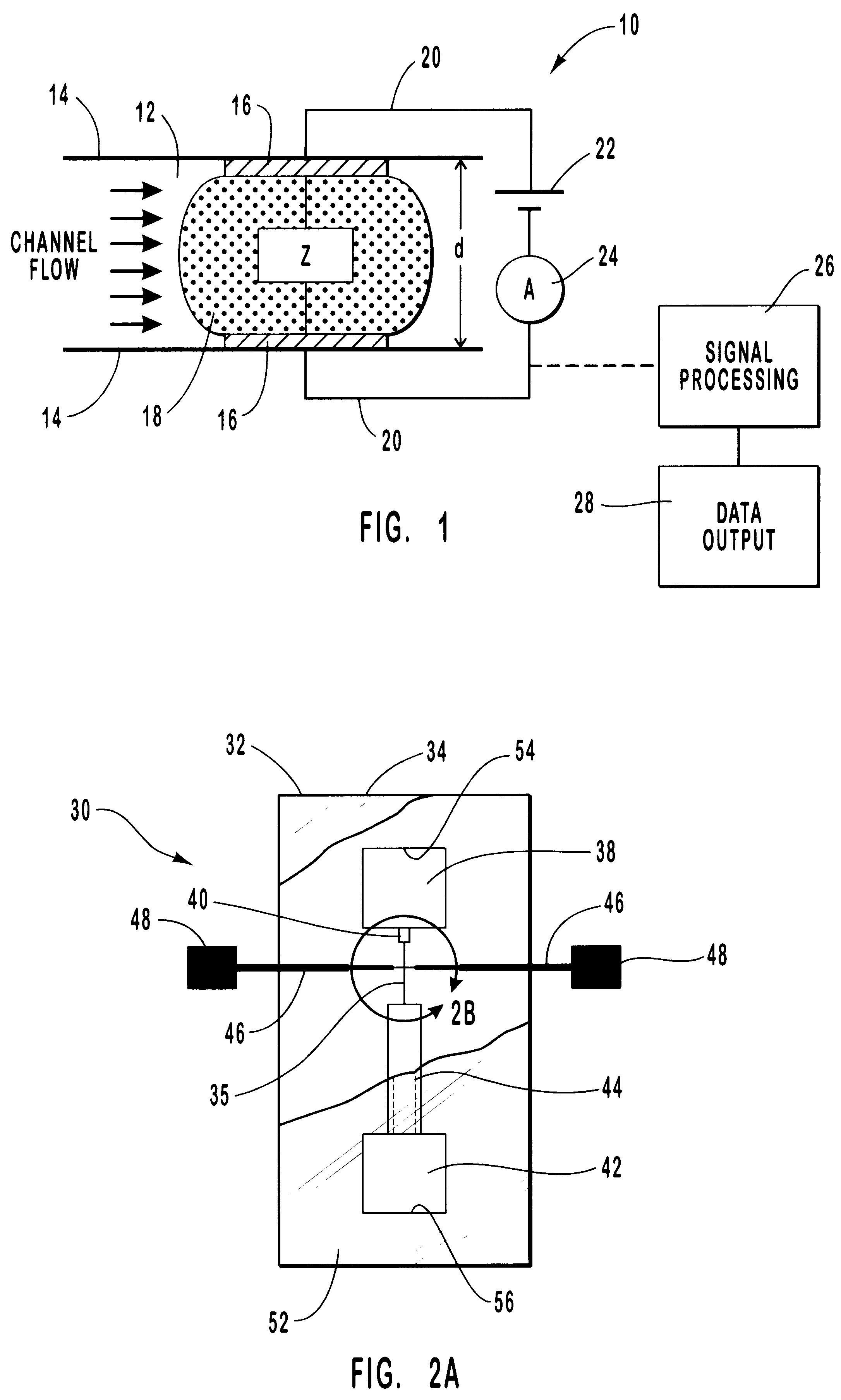
Two electrode MEI sensor devices were fabricated utilizing micromachining techniques. The sensor devices had small rectangular microchannels with typical cross-sectional areas of about 30 .mu.m.sup.2. Epoxy-based photoresist was used to form cell suspension reservoirs and the sidewalls of the microchannels in a glass substrate. Gold electrodes were electroplated to instrument the microchannels with a detection zone and had electrode tips with a cross-sectional area of about 20 .mu.m.sup.2. Glass coverslips with rectangular access holes were attached over the top of the microchannels.

The overall electrical impedance (Z) of the devices was measured between the gold electrode tips at frequencies swept in the range from 100 Hz to 2 MHz using an HP 4194 network analyzer from Hewlett-Packard (HP). The measured impedance is a function of the geometry and properties of the devices, as well as the interactions in the cell / media in the detection zone. The devices were characterized b...

Example

EXAMPLE 3

Microchannel devices for use in .mu.-EFFF systems were fabricated by the following procedure. A 3 inch (76 mm) single-side polished silicon wafer ( crystallographic orientation) was put into a PE-CVD apparatus and a layer of silicon nitride having a thickness of 2500 .ANG. was deposited on the polished side of the wafer. The silicon nitride was then patterned using photoresist as a mask on both sides of the wafer. Patterning was done such that 1 mm square openings were made in the silicon nitride on the unpolished side of the wafer in a CF.sub.4 plasma. Bulk anisotropic etching was then performed in a 20% KOH solution at a temperature of 56.degree. C. for a period of 24 hours to define the inlet and outlet ports. The KOH etching process left a thin silicon nitride membrane about 1000-2000 .ANG. thick on the front polished side of the wafer. The openings on the polished side of the wafer were about 200 square .mu.m.

Next, a layer of 1000 .ANG. of titanium followed by a layer ...

Example

EXAMPLE 4

Microchannel devices fabricated according to the procedure of Example 3 were tested for various characteristics. The microchannels used in these experiments were 6 mm in width and had a height of 26 .mu.m. The ends of the microchannels tapered to the inlet and outlet ports at a 60.degree. angle. All devices tested had a 25 .mu.m detector electrode on the silicon substrate. Once the microchannel and detector were fabricated, they were connected to an HP 6128C DC Power Supply and an HP 3458A multimeter. The multimeter was connected to a PC for data collection and analysis using LabView software. Connections, sample injection, pumps, and other hardware were also implemented to form an operative .mu.-EFFF system. The buffer solution used was deionized water for all experiments.

The experimental matrix took into account the variation of three basic parameters: buffer flow rate, applied voltage and corresponding current, and sample size and composition. Flow rates through the dete...


PUM


Abstract

A micro-electric detector provides conductivity or impedance based measurements of a test sample placed in a microchannel of a micro-analysis system. The detector includes a pair of electrodes disposed on opposing sidewalls of the microchannel to create a detection zone in the microchannel between and adjacent to the electrodes. A variety of test samples can be monitored by the detector, such as particulate-containing fluids and biological materials including living cells and subcellular structures. The detector can be integrated on-chip using micromachining techniques with a variety of micro-analysis systems.

Description

1. The Field of the InventionThe present invention relates generally to detector systems for measurement of the electrical characteristics of liquids, gases and biological materials. More specifically, the present invention relates to an electrical detector for micro-analysis systems capable of providing conductivity or impedance based measurements on a microscale of particulates in liquids or gases, and biological materials such as living cells.2. The Relevant TechnologyThe electrical properties of cells, organelles, and protein solutions are of fundamental interest in the fields of biophysics, physiology, biotechnology, and medicine. Various electrical properties have previously been studied by a variety of methods such as pipette, dielectrophoretic, or electrorotational methods.In the case of living organisms, pipette based methods suffer the disadvantage of being inherently invasive and require access to the intracellular space. Dielectrophoresis (DP) and electrorotation (ER) ar...

Claims


Application Information

Patent Timeline
IPC IPC(8): G01N30/00G01N27/447G01N30/64G01N15/14G01N30/60
CPCG01N27/4473G01N27/44791G01N30/64G01N15/14G01N30/0005G01N30/6095
Inventor FRAZIER, A. BRUNORABBITT, RICHARD D.AYLIFFE, H. EDWARD
Owner UTAH RES FOUND UNIV OF THE
Why Eureka
Try Eureka