Manufacturing method for semiconductor gas-phase epitaxial wafer

a manufacturing method and semiconductor technology, applied in semiconductor/solid-state device manufacturing, basic electric elements, electric devices, etc., can solve the problems of insufficient oxygen outward diffusion, high speed of silicon semiconductor device integration, and increasing demands on silicon wafer characteristics

Inactive Publication Date: 2001-04-03
SUMITOMO MITSUBISHI SILICON CORP
View PDF4 Cites 7 Cited by
  • Summary
  • Abstract
  • Description
  • Claims
  • Application Information

AI Technical Summary

Problems solved by technology

The large-scale integration of silicon semiconductor devices is progressing with high speed, and the characteristics required of silicon wafers have become increasingly more demanding.
Consequently, there is not enough outward diffusion of oxygen, and it is becoming difficult to curb the generation of crystal defects in the device active area.
This is a problem in that the aggregated silicon falls off the wafer surface in the semiconductor...

Method used


Image

  • Manufacturing method for semiconductor gas-phase epitaxial wafer
  • Manufacturing method for semiconductor gas-phase epitaxial wafer

Examples


embodiment 1

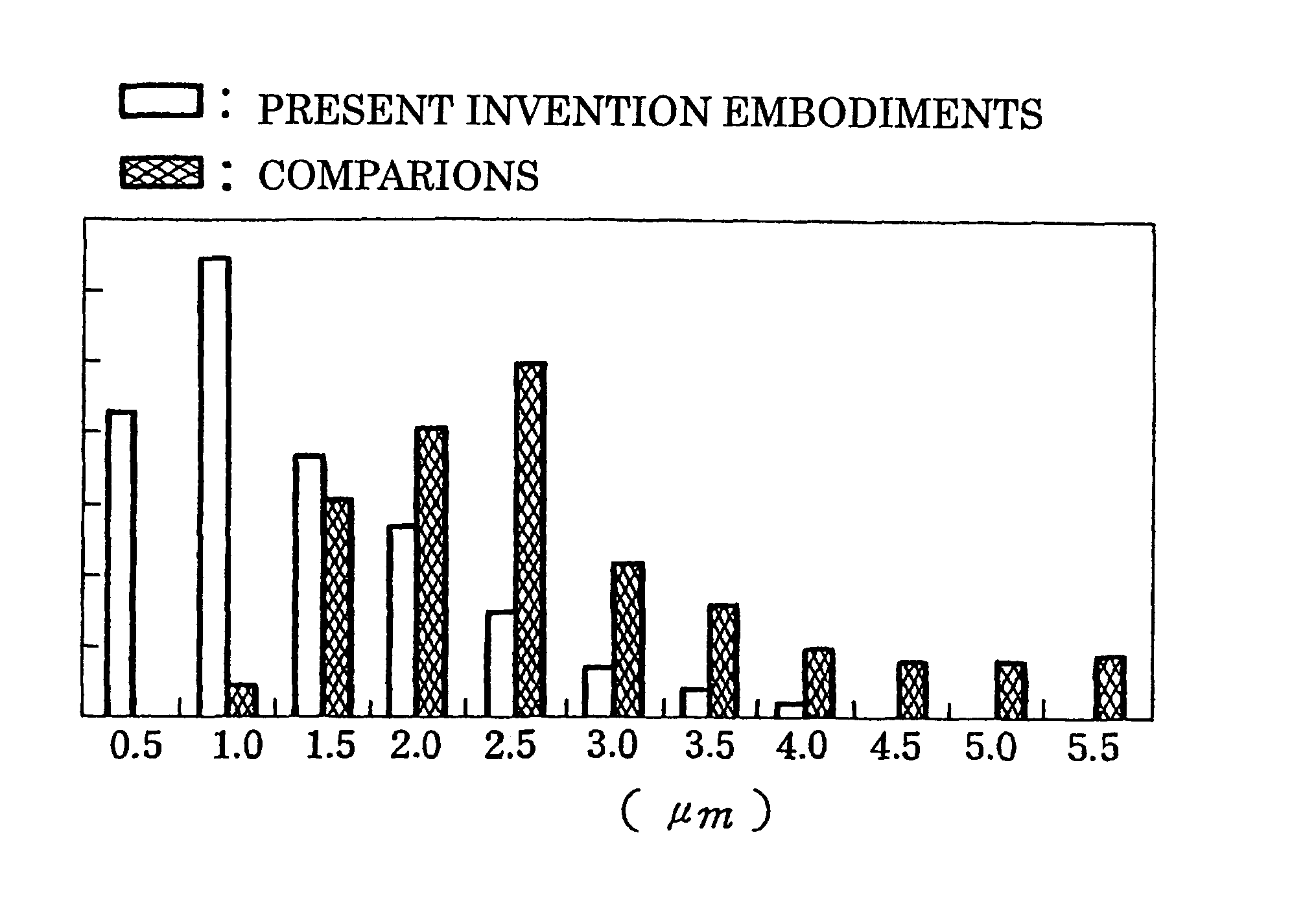
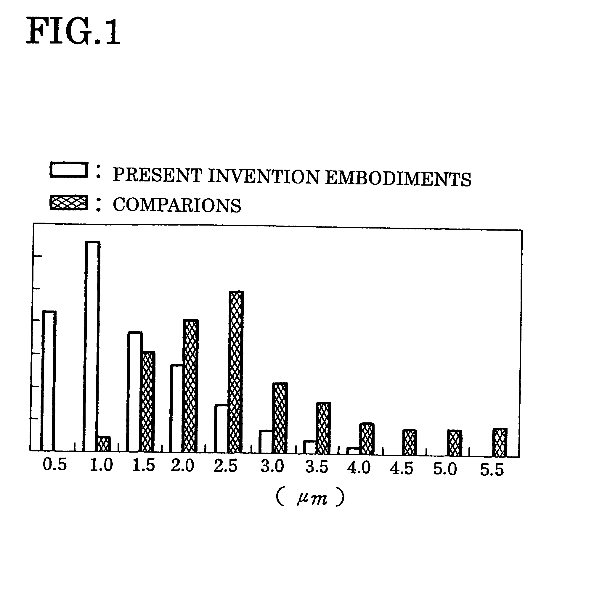
A 12-inch diameter CZ silicon wafer, which had undergone a slicing process and a flat grinding process, was subjected to polishing to remove around 10.about.30 .mu.m from both the front and back sides of the wafer, using a two-sided mirror-finish polishing apparatus. After which, a CVD film was grown on the backside of the wafer, the CVD film was removed from the edge-contoured portion, and the main surface of the wafer was finished by one-sided mirror-finish polishing using two-sided mirror-finish polishing apparatus to remove around 2 .mu.m. The flatness of 100 wafers thus produced was measured using an electrostatic capacity-type sensor, and a laser displacement gauge. The flatness variations thereof are shown in FIG. 1.

Compararison 1

A 12-inch diameter CZ silicon wafer, which had undergone a slicing process and an edge contouring process, was subjected to a lapping process. After which, the backside was etched, and a CVD film was grown on the backside. Then the CVD film was remov...

embodiment 2

When a CVD film and thermal oxide film are formed on the backside of a wafer that has been polished on both sides, the above-mentioned film is also formed on the peripheral surface of the wafer, where Si aggregates are readily formed. Embodiment 2 makes it possible to remove the above-mentioned film, which is formed either on this wafer peripheral surface, or for about 0.about.5 .mu.m toward the backside of the wafer from the peripheral surface, and furthermore, makes it possible to clamp a wafer in a rotating drive shaft chuck, and to remove the film from the peripheral surface of the wafer, and from the above-mentioned range of the in-plane portion by applying a head with a built-in non-woven fabric cloth impregnated with etchant to the film to be removed from the peripheral surface and other portions of the wafer while rotating the wafer around the drive shaft. It was ascertained that the same effect as that of the first embodiment is achieved.

embodiment 3

Embodiment 3 clamps a wafer in a rotating drive shaft chuck, and removes the film from the peripheral surface of the wafer, and from the above-mentioned range of the in-plane portion by applying a head with a built-in abrasive grain-holding tape film to the film to be removed from the peripheral surface and other portions of the wafer while rotating the wafer around the drive shaft. It was ascertained that the same effect as that of the first embodiment is achieved.


PUM


Abstract

The present invention has as an object, the provision of a manufacturing method for a semiconductor gas-phase epitaxial wafer which achieves the extremely high wafer flatness demanded in line with making wafers larger in size and heightening device process integration levels, and which forms either a backside CVD film or a thermal oxide film required as a gas-phase epitaxial wafer, and solves problems related thereto. More particularly, it achieves the high flatness and low processing deformation required by a large-diameter wafer, and makes it possible to enhance yield in the device process. In a manufacturing method for a semiconductor gas-phase epitaxial wafer, which enables a thin, disc-shaped wafer to be sliced from a single-crystal ingot, a required surface to be finished to a mirror surface, and an epitaxial layer to be formed on the main surface, that introducing into the above-mentioned manufacturing method a two-sided polishing process for polishing both the front and back surfaces of a wafer; a process for forming either a CVD film or a thermal oxide film on the backside of a wafer; and a one-sided mirror-finish polishing process for polishing the main surface of a wafer enables the realization of the extremely high wafer flatness demanded by a large-diameter wafer, while preventing autodoping.

Description

The present invention relates to a manufacturing method for a semiconductor gas-phase epitaxial wafer, having a silicon epitaxial layer, which is grown on a main surface of a wafer, and used as a substrate for circuit elements of LSI (large-scale integration). More specifically, the present invention relates to a manufacturing method for a semiconductor gas-phase epitaxial wafer. In which a two-sided polishing process, a wafer backside CVD film growth process, and a one-sided polishing process, which polishes the main surface, are performed when preparing a wafer for epitaxial growth, thereby achieving extremely outstanding flatness, and a large-diameter with particularly high precision, and therefore increasing the precision and quality of the silicon epitaxial layer grown thereafter.DESCRIPTION OF THE PRIOR ARTThe large-scale integration of silicon semiconductor devices is progressing with high speed, and the characteristics required of silicon wafers have become increasingly more...

Claims


Application Information

Patent Timeline
IPC IPC(8): H01L21/02H01L21/304H01L21/3105H01L21/205H01L21/316
CPCH01L21/304H01L21/31053
Inventor MASUDA, SUMIHISASAKAI, MASATO
Owner SUMITOMO MITSUBISHI SILICON CORP
Why Eureka
Try Eureka