Semiconductor device and fabrication method thereof

a technology of semiconductor devices and semiconductors, applied in semiconductor devices, instruments, optics, etc., can solve the problems of difficult to provide an element having sufficient function with operational speed, difficult to control the ldd region for these, and severe operation functions requested to

Inactive Publication Date: 2001-04-17
SEMICON ENERGY LAB CO LTD
View PDF22 Cites 233 Cited by
  • Summary
  • Abstract
  • Description
  • Claims
  • Application Information

AI Technical Summary

Problems solved by technology

However, high function formation of AMLCD has been progressed year by year and operational function (particularly, operational speed) requested to TFT tends to become severe.
Therefore, it is difficult to provide an element having sufficient function with operational speed of TFT using an amorphous silicon film.
First, a total of an active layer is extremely thin to about 50 nm and accordingly, impact ionization is caused at a junction between a channel forming region and a drain region and deteriorating phenomena of hot carrier injection and the like significantly emerge. Therefore, there causes a necessity of forming a large LDD region (Light Doped Drain Region).
Further, controllability of the LDD region for these is the most important problem.
In an LDD region, control of a concentration of impurities and a length of the region is very delicate and particularly, control of length becomes problematic.
At current state, a system for prescribing a length of an LDD region by a mask pattern is adopted, however, when miniaturization is promoted, slight patterning error causes a significant difference in properties of TFT.
A variation in sheet resistance of an LDD region caused by a variation in a film thickness of an active layer poses a serious problem.
Further, a patterning step is needed to form an LDD region which gives rise to an increase in fabrication steps as it is and a deterioration in throughput.
As mentioned above, according to an inverted stagger structure of a channel stop type, LDD regions must be formed on both sides of a channel forming region and in a plane in the horizontal direction and it is very difficult to form a reproducible LDD region.

Method used


Image

  • Semiconductor device and fabrication method thereof
  • Semiconductor device and fabrication method thereof
  • Semiconductor device and fabrication method thereof

Examples


embodiment 1

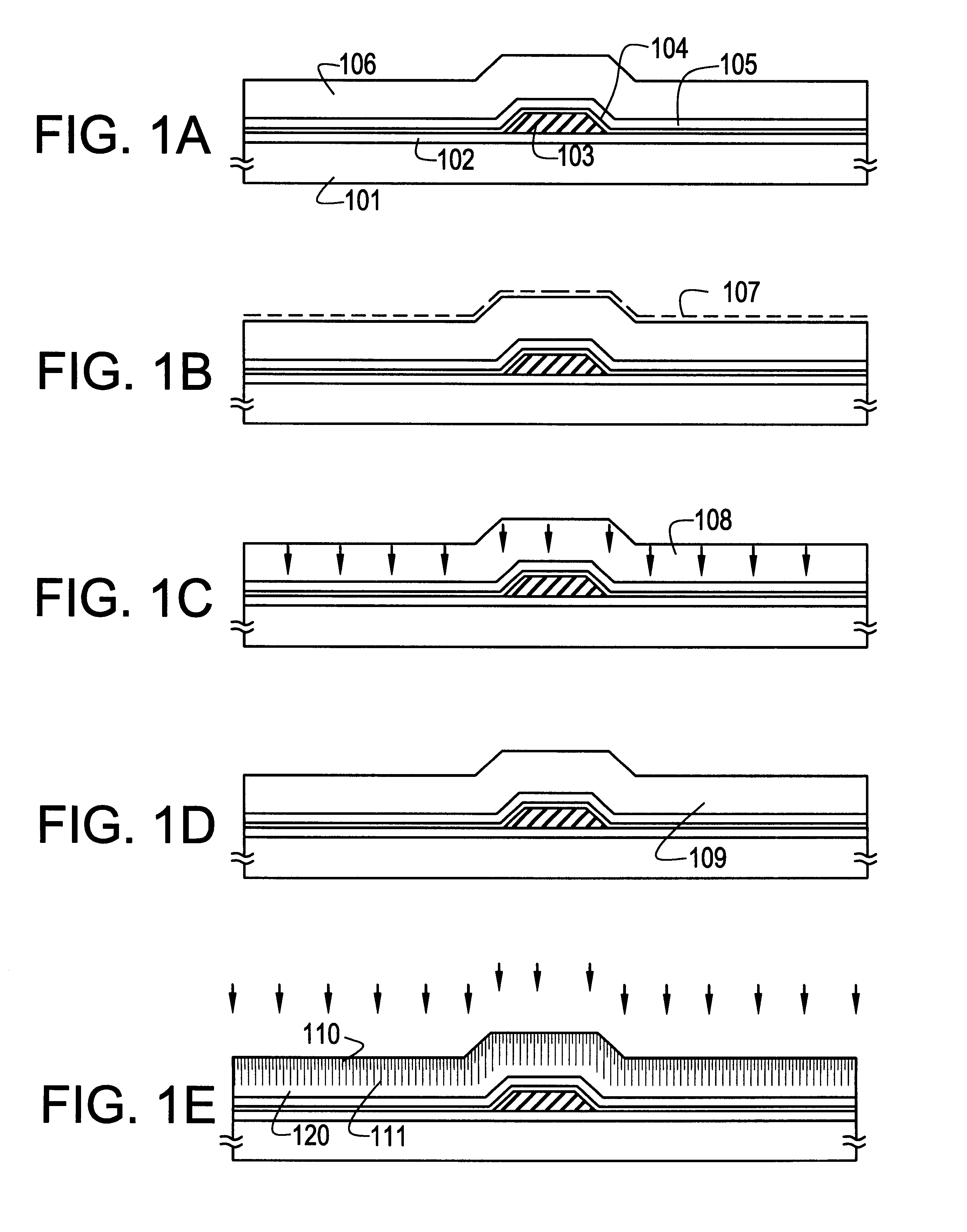
An explanation will be given of a representative embodiment according to the present invention in reference to FIGS. 1A-1E, 2A-2D and 3. First, an explanation will be given of a method of fabricating a semiconductor device according to the present invention in reference to FIGS. 1A-1E.

A base film 102 comprising an insulating film whose major component is silicon is formed on a glass substrate (or quartz, silicon substrate) 101. On top thereof, a gate electrode (first wiring) comprising a conductive film 103 is formed.

A line width of the gate electrode 103 is set to 1-10 .mu.m (representatively, 3-5 .mu.m). Further, the film thickness is set to 200-500 nm (representatively, 250-300 nm). In this embodiment, a gate electrode having a line width of 3 .mu.m is formed by using a Ta / TaN (tantalum / tantalum nitride) laminated layer film having a thickness of 250 nm.

Further, a material having heat resistance withstanding temperature of at least 600.degree. C. (preferably, 800.degree. C.) (tan...

embodiment 2

This embodiment is an example of crystallizing an amorphous silicon film by laser without using a catalyst element in Embodiment 1. An explanation will be given of a representative embodiment of the present invention in reference to FIGS. 5A-5D, 6A-6C and 7.

The line width of a gate electrode 203 is set to 1-10 .mu.m (representatively, 3-5 .mu.m). Further, the film thickness is set to 200-500 nm (representatively, 250-300 nm). According to the embodiment, a gate electrode having the line width of 3 .mu.m is formed by using an aluminum film (including 2 wt % of scandium) having a thickness of 250 nm.

Further, other than aluminum, the gate electrode 203 can use tantalum, tungsten, titanium, chromium, molybdenum, conductive silicon, metal silicide, laminated layer films of these and so on. At this stage, a first patterning step (gate electrode formation) is carried out.

At this stage, the gate electrode 203 is anodized and an anodic oxide film 204 for protecting the gate electrode is form...

embodiment 3

According to the embodiment, in the constitution of the present invention, an example of a constitution different from those of Embodiments 1 and 2 will be shown. The fabrication steps of TFT are basically carried out in accordance with those in Embodiments 1 and 2 and accordingly, in this embodiment, an explanation will be given only of necessary portions.

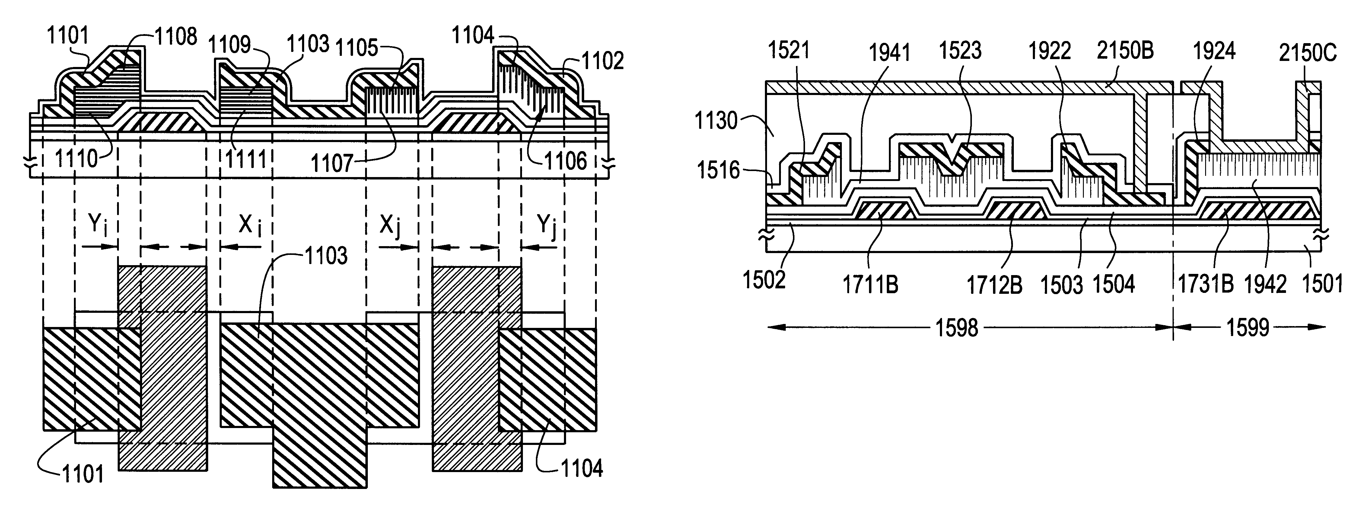
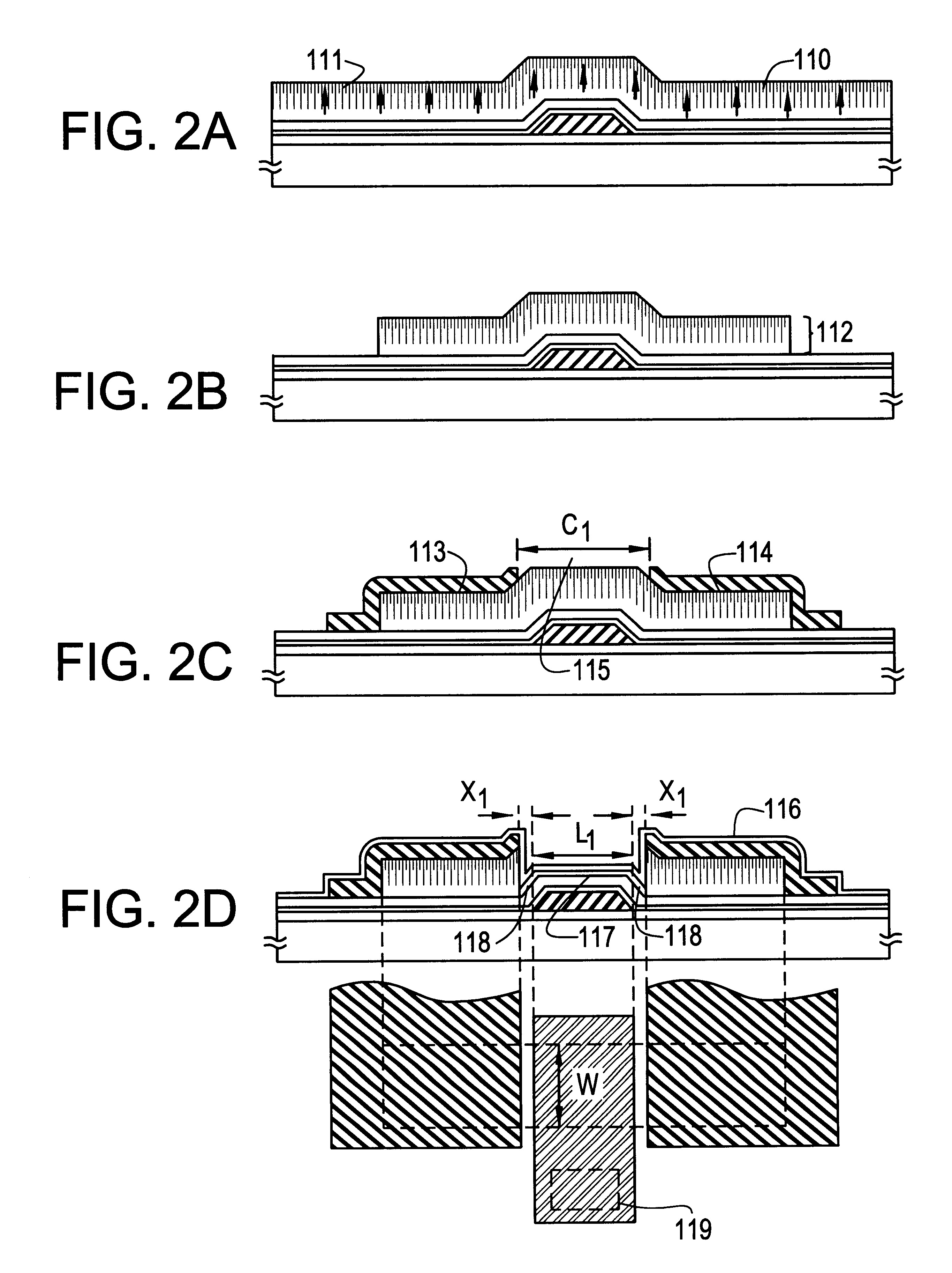
First, a state of FIG. 8A is provided in accordance with the fabrication steps of Embodiment 1 or Embodiment 2. In this case, a point different from Embodiments 1 and 2 resides in that a length of a channel etch region 800 is set to C.sub.2 in forming a source electrode 801 and a drain electrode 802. In this case, C.sub.2 is narrower than the width of the gate electrode and is selected in a range of 2-9 .mu.m (representatively, 2-4 .mu.m). It is the characteristic of this embodiment to provide a gate electrode and source and drain electrodes to overlap each other.

When the channel etch step is carried out as shown by Embodiment 1 o...


PUM

PropertyMeasurementUnit
widthaaaaaaaaaa
widthaaaaaaaaaa
thicknessaaaaaaaaaa

Abstract

To provide a semiconductor device having high mass production performance and high reliability and reproducibility by simple fabrication steps, in a constitution of a semiconductor device of a bottom gate type formed by a semiconductor layer having a crystal structure, source and drain regions are constituted by a laminated layer structure comprising a first conductive layer (n+ layer), a second conductive layer (n- layer) having resistance higher than the first conductive layer and an intrinsic or a substantially intrinsic semiconductor layer (i layer) in which the n- layer functions as an LDD region and the i layer functions as an offset region in a film thickness direction.

Description

1. Field of the InventionThe present invention relates to a semiconductor device utilizing a semiconductor thin film having a crystal structure and a fabrication method thereof. Particularly, the present invention relates to a semiconductor device using a thin film transistor (hereinafter, abbreviated as TFT) having an inverted stagger structure.Further, "semiconductor device" in the specification designates all of devices operated by utilizing semiconductor properties. Accordingly, all of TFTs, AMLCDs (Active Matrix Type Liquid Crystal Display Device) and electronic devices described in the specification are included in the category of semiconductor devices.2. Description of Related ArtConventionally, there has been utilized TFT as a switching element of an active matrix type liquid crystal display device (hereinafter, abbreviated as AMLCD). Currently, a product constituting a circuit by TFT utilizing an amorphous silicon film as an active layer is predominant in the market. As str...

Claims


Application Information

Patent Timeline
Patent Type & Authority Patents(United States)
IPC IPC(8): G02F1/13G02F1/1362H01L21/02H01L21/336H01L21/70H01L29/66H01L27/12H01L21/84H01L29/786H01L21/328H01L21/20H01L21/77H01L27/13
CPCG02F1/136213H01L29/66765H01L29/78618H01L27/1255H01L27/1277G02F1/136227H01L21/02532H01L21/02672H01L21/02686H01L21/02691H01L27/12H01L27/1214H01L27/13
Inventor YAMAZAKI, SHUNPEIKOYAMA, JUNSATOU, YURIKA
Owner SEMICON ENERGY LAB CO LTD
Why Eureka
Try Eureka