

Semiconductor device having impurity region locally at an end of channel formation region
Inactive Publication Date: 2001-05-15
SEMICON ENERGY LAB CO LTD
View PDF40 Cites 57 Cited by
- Summary
- Abstract
- Description
- Claims
- Application Information
AI Technical Summary
Benefits of technology
When a region where carriers move is intrinsic or substantially intrinsic, the reduction of mobility attributable to impurity scattering is quite small. This is a significant advantage of the invention which suppresses or prevents the short channel effect without using channel doping.
which suppresses or prevents the short channel effect without using channel doping.
The reason is that a conventional IC is doped with impurities on the entire surface of the channel formation region using channel doping. This creates a problem in that only low mobility (field effect mobility) is achieved in spite of the use of single crystal because of impurity scattering.
In the pinning FET according to the present invention, pinning regions are locally provided relative to the channel formation region to prevent the short channel effect and to control the threshold voltage. As a result, the region where carriers move becomes an intrinsic or substantially intrinsic region to provide high mobility.
A fourth effect will now be described. While it has been already described that pinning regions according to the invention have a function of preventing the short channel effect and controlling the threshold voltage, they also play a very important role in preventing a decrease in the withstand voltage between the source and drain due to impact ionization.
As described with reference to the prior art, minority carriers (holes in the present embodiment) generated by impact ionization can cause breakdown phenomena induced by carrier implantation such as conduction of a parasitic bipolar transistor and a decrease in the diffusion potential near the source as a result of the accumulation of the minority carriers in the vicinity of the source.
Problems solved by technology
However, a phenomenon referred to as "short channel effect" is known as a factor which hinders semiconductor devices from being made finer.
The short channel effect represents various problems such as a decrease in a withstand voltage between a source and a drain and a decrease in a threshold voltage which occur as a result of a decrease in a channel length.
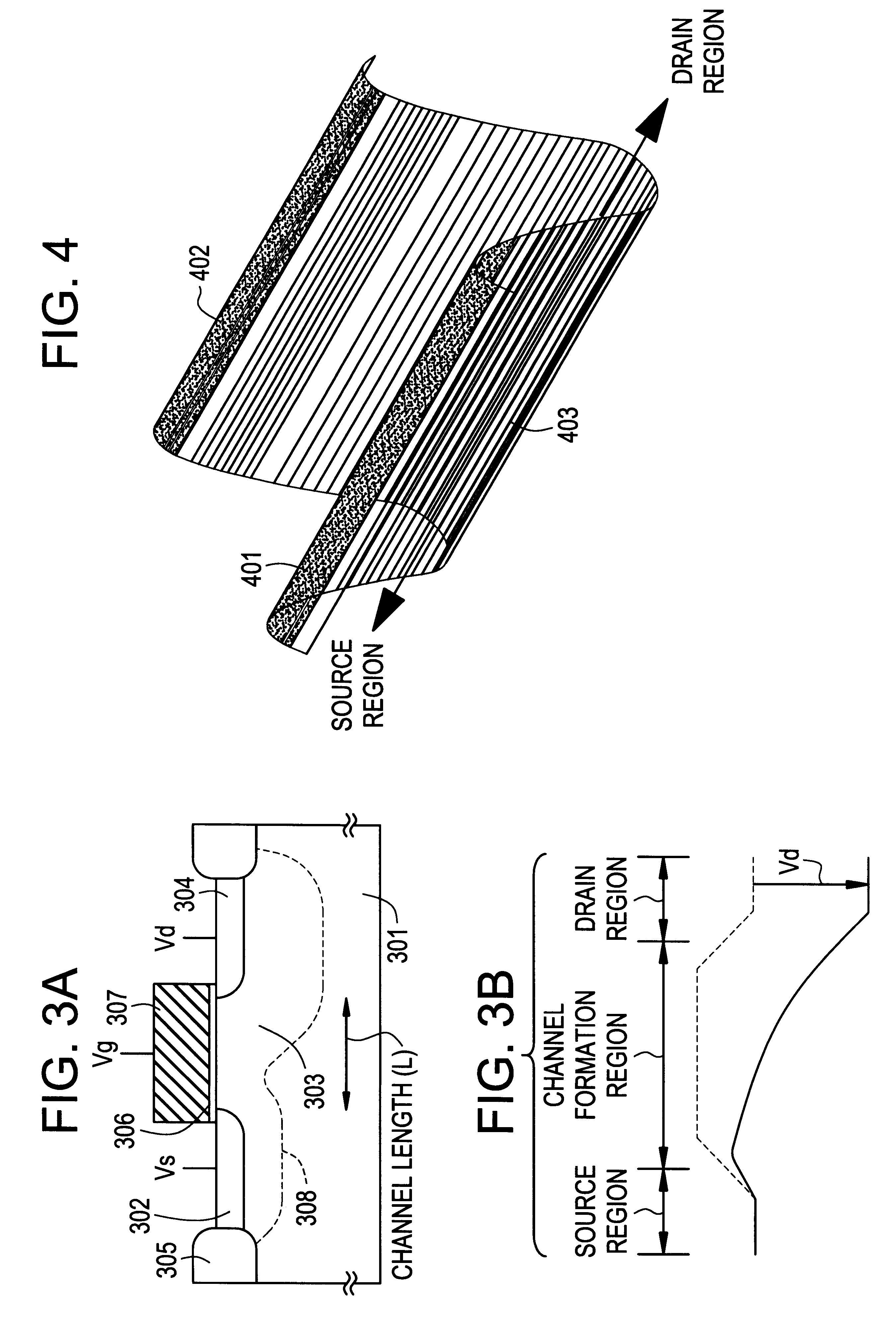
According to this article, one of the most commonly known causes of a decrease in a withstand voltage is punch-through which is a phenomenon wherein, as a result of a decrease in a channel length, electric potential at a depletion layer toward the drain (referred to as "drain-side depletion layer) affects a region toward the source to decrease diffusion potential near the source (drain-induced barrier reduction), thereby making it difficult to control carriers using a gate voltage.
As a result, a potential barrier in the vicinity of the source is decreased by the drain voltage to cause an unintended flow of a current even when no gate voltage is applied.
There is a phenomenon called "impact ionization of implanted carriers" which is another cause of a decrease in the withstand voltage between the source and drain.
Those holes cause a breakdown phenomenon induced by the implantation of the carriers.
However, channel doping has a problem in that it places a significant limitation on field effect mobility of a MOSFET (hereinafter simply referred to as "mobility").
Specifically, an intentionally added impurity element interferes with the movement of the carries to reduce the mobility of the same.
Further, it is difficult to achieve the pinning effect with a channel width in the excess of 500 nm.
This creates a problem in that only low mobility (field effect mobility) is achieved in spite of the use of single crystal because of impurity scattering.
Meanwhile, the narrow channel effect also tends to increase the threshold voltage, which results in a considerable increase in the absolute value of the threshold voltage.
That is, it is not suitable for cases wherein source and drain regions are periodically switched as encountered in a pixel transistor for an active matrix type display.
However, a buried channel type FET has a problem in that it has low withstand voltage characteristics because it is vulnerable to punch-through.
Method used
View moreImage
Smart ImageViewing Examples

Examples
Embodiment Construction
is provided for the purposes of illustration and is not intended to be exhaustive or to limit the invention to the precise embodiment disclosed. Accordingly, the scope of the present invention is defined by the appended claims.
Login to View More PUM
 Abstract
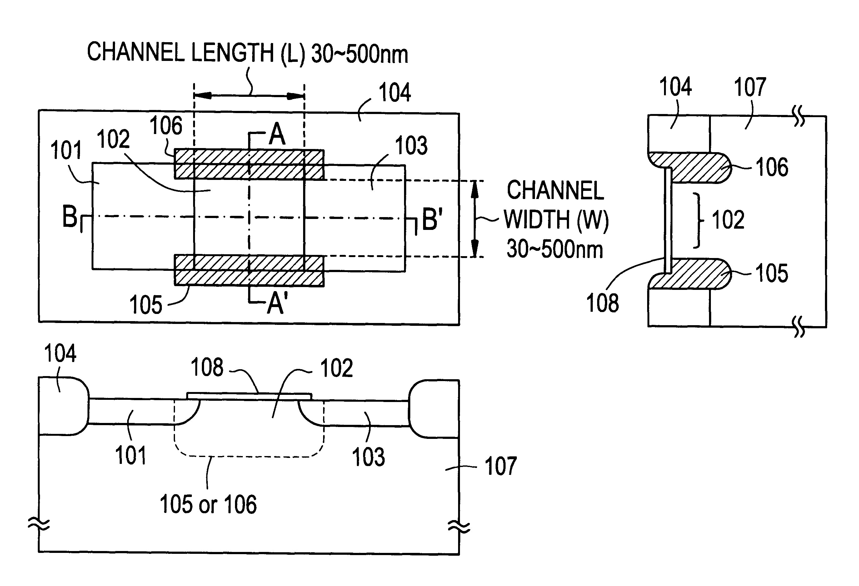
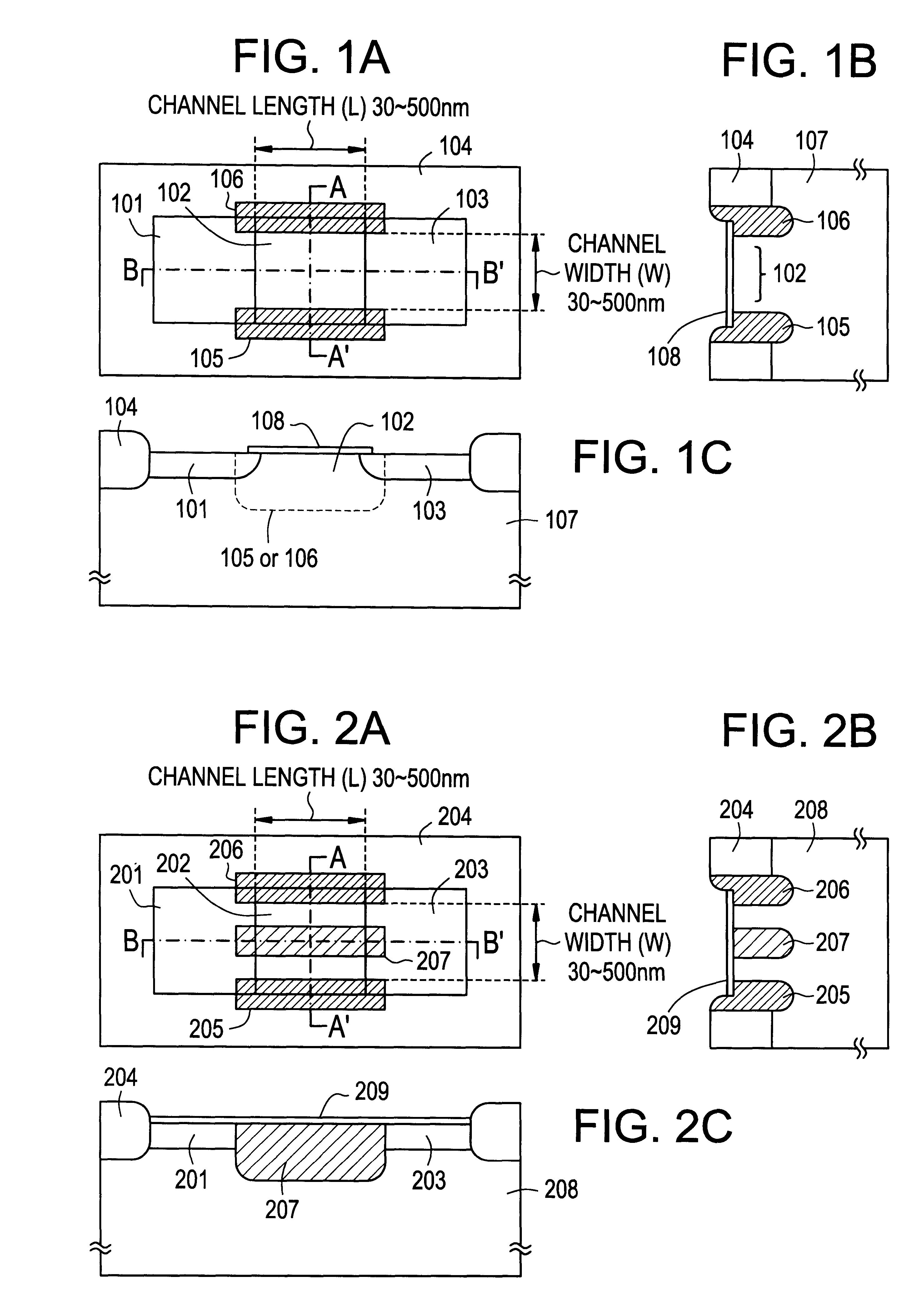
There is provided a semiconductor device having a novel structure in which high reliability and high field effect mobility can be simultaneously achieved. In an insulated gate transistor formed on a single crystal silicon substrate, pinning regions 105 and 106 are formed at the ends of a channel formation region 102. The pinning regions 105 and 106 suppress the expansion of a depletion layer from the drain side to prevent a short channel effect. In addition, they also serve as a path for extracting minority carriers generated as a result of impact ionization to prevent breakdown phenomena induced by carrier implantation.
Description
1. Field of the InventionThe present invention relates to a semiconductor device formed using a single crystal silicon substrate and, more particularly, to a configuration of an insulated gate field effect transistor (referred to as "MOSFET" or "IGFET").The present invention is a technique which is effective for the fabrication of a fine device having a channel length and a channel width equal to or less than 1 .mu.m (typically in the range from 30 to 500 nm).The present invention can be applied to various semiconductor integrated circuits such as ICs, VLSIs and ULSIs which are formed by integrating MOSFETs.2. Description of the Related ArtRecently, integrated circuits such as VLSIs are becoming increasingly finer, which has resulted in a need for processing dimensions in a deep submicron domain wherein the channel length (L) of a MOSFET is 0.2 .mu.m or less, more preferably, 0.1 .mu.m or less.Similarly, processing dimensions as fine as 0.2 .mu.m or less are also required for the ga...
Claims
Login to View More Application Information
Patent Timeline
 IPC IPC(8): H01L21/70H01L29/78H01L21/8238H01L29/10H01L29/66H01L29/02
CPCH01L21/823807H01L21/823878H01L29/1041H01L29/1045H01L29/7838H01L2924/0002H01L2924/00
InventorYAMAZAKI, SHUNPEI
OwnerSEMICON ENERGY LAB CO LTD