Precise endpoint detection for etching processes

a technology of etching process and endpoint detection, which is applied in the field of etching process precision, can solve the problems of reducing the accuracy with which the process may be controlled, increasing the uncertainty as to the progress of the etching process, and relative high process speed

Inactive Publication Date: 2001-07-10
IBM CORP
View PDF16 Cites 33 Cited by
  • Summary
  • Abstract
  • Description
  • Claims
  • Application Information

AI Technical Summary

Problems solved by technology

However, the relatively high speed of the process decreases the accuracy with which the process may be controlled.
Further, the reactive ion etch process generally take a short but variable time to stabilize, once started, which increases the uncertainty as to the progress of the etching process.
This accuracy is insufficient to support the desired degree of consistency of integrated circuit element performance or even consistently high yield.
This approach, however, does not provide a solution to the above problem since the etched material is entirely removed and the etch stop material may not have the desired electrical properties.
This approach has several significant drawbacks, however.
The developmen

Method used


Image

  • Precise endpoint detection for etching processes
  • Precise endpoint detection for etching processes
  • Precise endpoint detection for etching processes

Examples


Embodiment Construction

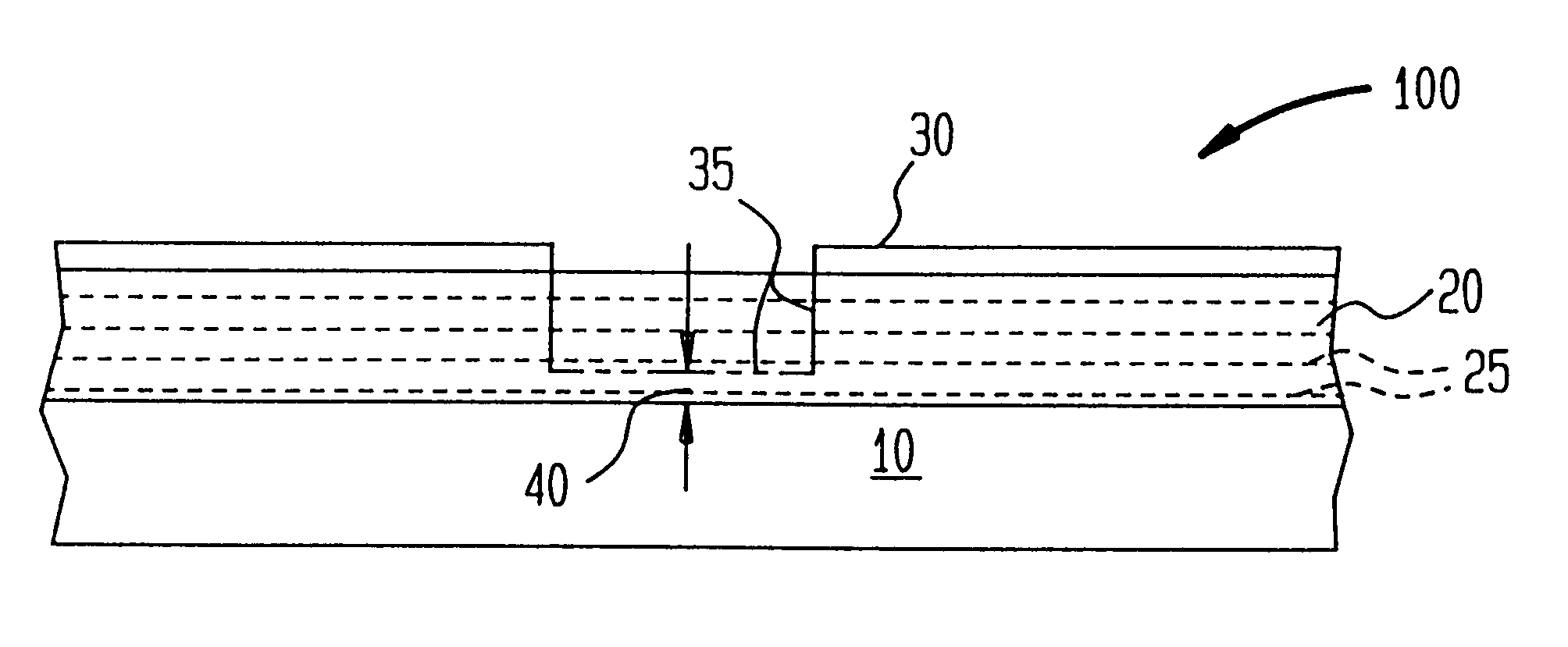
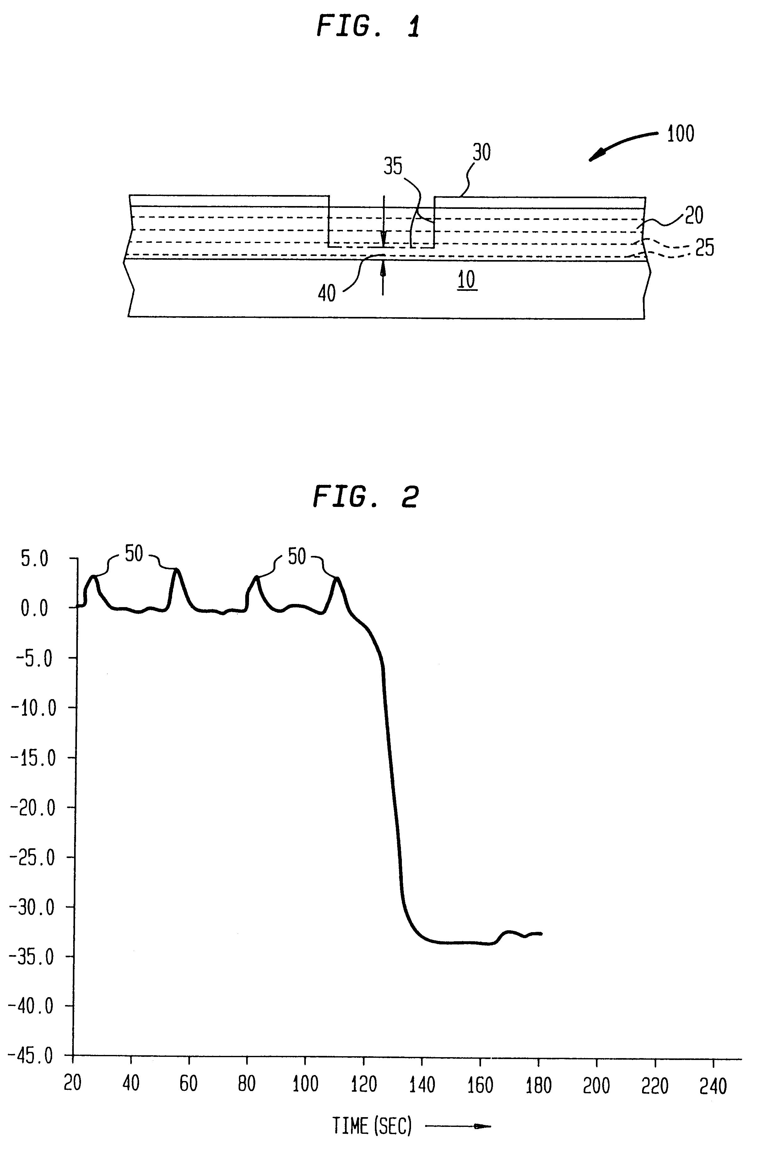
Referring now to the drawings, and more particularly to FIG. 1, there is shown a cross section of a structure 100 upon which etching is to be performed in accordance with the present invention. This structure comprises a layer 20 to be etched over an underlying layer 10 and a mask 30 which defines the lateral extent of the etching. The region of layer 20 to be etched away is shown by chain line 35 and leaves a thin region 40 of layer 20. The particular materials of layers 10 and 20 are not important to the principles or practice of the invention. However, in the presently contemplated applications of the invention, region 40 may form the base of a bipolar transistor, in which case layer 20 could be polysilicon, or the gate insulator of a field-effect transistor, in which case layer 20 would be an insulator such as silicon oxide. The thickness of such a layer is critical to performance in both of these types of devices. Performance is degraded if the layer is of increased thickness a...


PUM

PropertyMeasurementUnit
Timeaaaaaaaaaa
Volumeaaaaaaaaaa
Depthaaaaaaaaaa

Abstract

A homogeneous marker is formed, possibly by the adsorption of trace amounts of an ambient material such as carbon monoxide gas, at a surface of a deposited material when the plasma in momentarily interrupted during plasma enhanced chemical vapor deposition or other deposition processes involving the presence of a plasma. When the deposited material is etched, the resulting crystal dislocations or adsorbed gas is detected as a marker by optical emission spectroscopy techniques. The accuracy of an end point determination of the etching process can be increased by providing a sequence of such markers within the bulk or volume of the deposited material. The markers, being merely an interface such as a slight crystal dislocation in otherwise homogeneous material, do not affect the electrical, chemical or optical properties of the remainder of the predetermined deposited material and thus the homogeneity of the deposited material is not significantly affected.

Description

1. Field of the InventionThe present invention generally relates to etching processes and, more particularly, to precision etching of deposited material in semiconductor structures.2. Description of the Prior ArtDue to the small size of elements of integrated circuits and the small minimum feature size of patterns of materials of which they are formed, many manufacturing process steps simultaneously deposit materials on or etch materials away from a plurality of masked areas over the entire surface of a chip or wafer. Many current, high performance semiconductor device designs also require the formation of layers of very precise thicknesses. Such thicknesses of material are usually formed by depositing a thicker layer and then etching it to the desired thickness. Such a technique allows more reliable formation of the layer which may not be continuous if merely deposited to the desired thickness.Among etching techniques, reactive ion etching (RIE) is very desirable due to its relativ...

Claims


Application Information

Patent Timeline
IPC IPC(8): H01L21/02H01L21/311H01L21/3065
CPCH01J37/32963H01L21/31116H01L21/3065
Inventor KROPP, LAWRENCE ANDREWSTANASOLOVICH, DAVIDWEISS, MARC JAYYEE, DENNIS SEK-ON
Owner IBM CORP
Why Eureka
Try Eureka