Methods for forming solder balls on substrates

a technology of substrate and solder ball, which is applied in the direction of soldering apparatus, manufacturing tools, non-printed masks, etc., can solve the problems of limiting the usefulness of the technique, high cost of metal mask replacement, and inability to meet the needs of fine pitch ball bumping, so as to reduce the effective thermal mass of the chuck assembly and reduce the effect of reflowed

Inactive Publication Date: 2001-09-25
SEMIPAC INC
View PDF65 Cites 48 Cited by
  • Summary
  • Abstract
  • Description
  • Claims
  • Application Information

AI Technical Summary

Benefits of technology

An additional advantage of the chuck assembly 900 is that the wafer 902 is disposed upon a non-metallic film 930 which, in turn, is disposed upon a non-metallic membrane 914, both of which (930 and 914) serve as thermal barriers to isolate the thermal mass of the chuck...

Problems solved by technology

A number of techniques are known for ball bumping electronic components, some of which are not well suited to fine pitch ball bumping.
This requires a high investment in capital equipment and has high cost associated with cleaning the processing equipment and with replacing the metal mask on a frequent basis.
Thermal mismatch between the evaporation mask and the substrate being ball bumped tends to limit the usefulness of the technique to moderate densities and moderate solder bump sizes.
This technique is time consuming, requires high capital expenditure, and involves hazardous chemicals.
This technique is relatively inexpensive, and comprises only a few quick steps, but is generally not well suited to small bump sizes and high bump densities.
The advent and popularity of the BGA package has brought with it several new package manufacturing and assembly problems.
One of the more significant problems is finding an efficient, cost-effective technique for applying the solder balls to the package surface.
Difficulties with any technique involving measuring or dispensing precise quantities of solder paste on pads to form ball bumps include dealing with the rheological characteristics (elasticity, viscosity, plasticity) of the solder paste, accurately controlling the volume of solder paste after dispensing and reflow, and the shape of the final ball bump.
As mentioned above, in general it is difficult to form contacts with height-to-width rati...

Method used


Image

  • Methods for forming solder balls on substrates
  • Methods for forming solder balls on substrates
  • Methods for forming solder balls on substrates

Examples


Embodiment Construction

OF SOLDER MATERIALS AND MASK DIMENSIONS

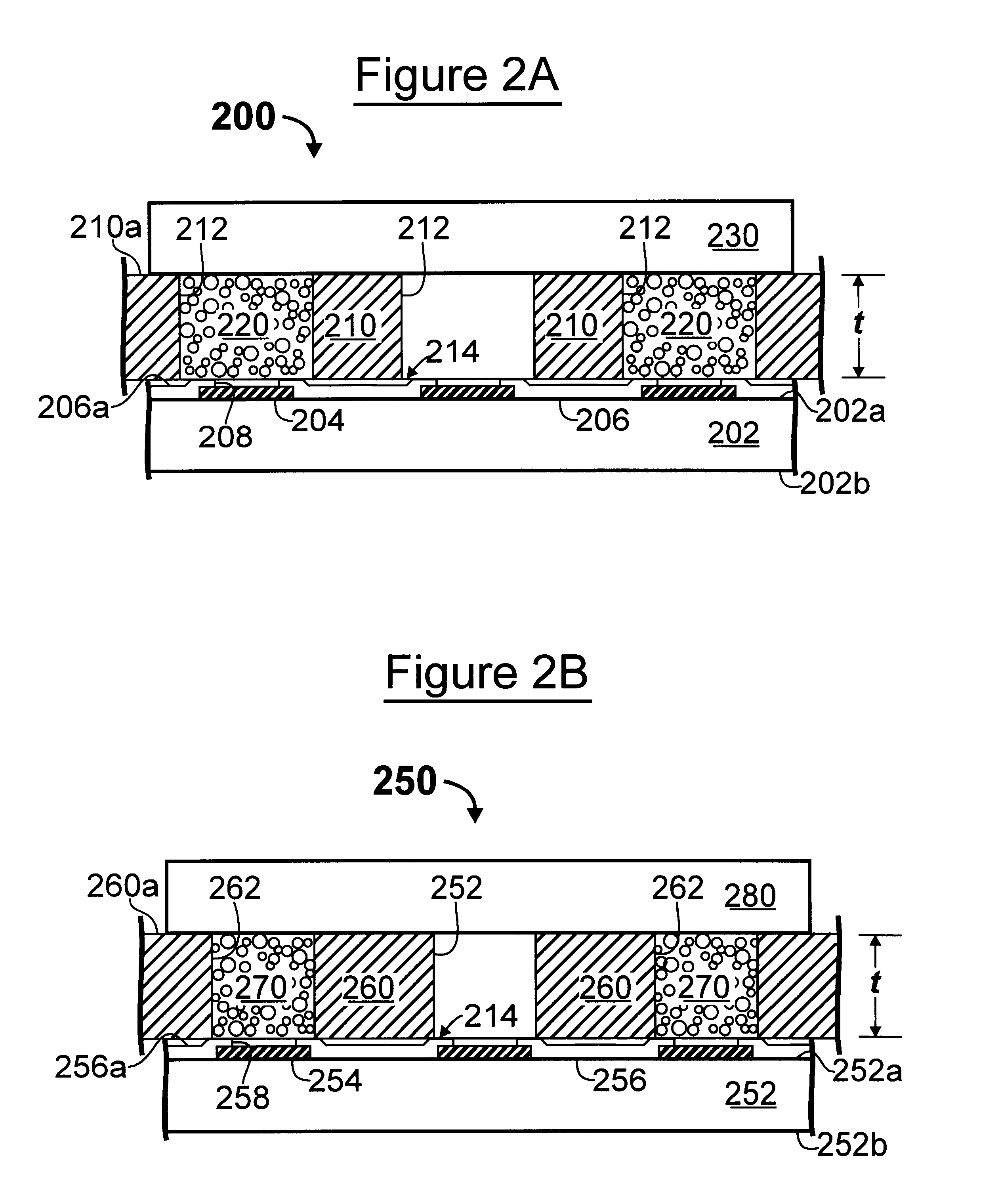
A suitable solder material for use with the present invention comprises "63 / 37" lead / tin solder having a melting temperature of approximately 183.degree. C. (Centigrade), and has relatively large particle sizes. Large solder particles are less likely to leak out of any gap (e.g., 314) between the mask and the substrate being bumped. The following chart lists a number of exemplary dimensions and relationships between:

D, the diameter of the desired resulting solder ball;

W, the cross-dimension of the cell in the mask;

T, the thickness of the mask;

d, the particle size (e.g., diameter);

#, the approximate number of particles in a cell; and

%, the final percentage of metal, by volume, in the cell.

From the chart presented above, it is evident that:

The cross-dimension (W) of a mask cell is always greater than the thickness (T) of the mask.

The solder material filling the cells in the mask preferably comprises solder particles which of a size (d) which is r...


PUM

PropertyMeasurementUnit
Temperatureaaaaaaaaaa
Pressureaaaaaaaaaa
Heataaaaaaaaaa

Abstract

A mask (110; see also 160, 210, 260, 310, 408, 500, 702, 802, 904) having a plurality of openings (cells) is disposed on, or nearly on, the surface of a substrate (102), the openings (112) of the mask being aligned over a corresponding plurality of pads (104) on the substrate. The openings in the mask are filled with solder material (114). A pressure plate (120) is disposed over the mask to capture the solder material in the cells. Heat is directed at the mask (through the pressure plate) to reflow the solder. This is done in an inverted or partially inverted orientation. The stackup (assembly) of substrate/mask/pressure plate may be un-inverted prior to cooling. Mask configurations, methods of mounting the masks, and solder material compositions are described. The methods are robust, and are well suited to fine pitch as well as coarse pitch ball bumping of substrates.

Description

The invention relates to methods of forming solder balls on substrates which are electronic components such as semiconductor devices (integrated circuit chips) and interconnection substrates, and to apparatuses for forming the solder balls on the electronic components. BACKGROUND OF THE INVENTIONIn recent years, flip-chip bonding techniques have increasingly been used to connect (bond) integrated circuit (IC) chips to interconnection substrates and to package substrates. In flip-chip bonding an IC chip component to an interconnection component such as ceramic interconnection substrate, a plurality (e.g., an array) of solder balls (also called "solder bumps") is formed on a face of a component, typically the IC chip component, and the bumped component is brought into a face-to-face relationship with the other component. The two components are then heated (such as in a furnace) to reflow (heat, then allow to cool) the solder bumps, thereby making electrical connections between respect...

Claims


Application Information

Patent Timeline
IPC IPC(8): B23K35/02B23K3/06H01L21/02H01L21/60H01L21/48H05K3/34B23K35/22B23K35/14
CPCB23K3/0623B23K35/0244H01L21/4853H01L24/11H05K3/3484B23K35/0222H01L2224/11334B23K35/224B23K2201/40H01L2224/11003H01L2224/13099H01L2924/01027H01L2924/01029H01L2924/01039H01L2924/01042H01L2924/01074H01L2924/01075H01L2924/01082H01L2924/14H05K2201/10477H05K2203/0113H05K2203/0278H05K2203/0338H05K2203/043H05K2203/0557H01L2924/01006H01L2924/01033H01L2924/014B23K2101/40H01L2224/05568H01L2224/05573H01L2924/00014H01L2924/351H05K3/3485H01L2924/00H01L2224/05599
Inventor MACKAY, JOHNMOLINARO, TOM
Owner SEMIPAC INC
Why Eureka
Try Eureka