Metallization structure on a fluorine-containing dielectric and a method for fabrication thereof

a technology of fluorine-containing dielectrics and metal structures, which is applied in the direction of basic electric elements, solid-state devices, electric devices, etc., can solve the problems of not being able to meet stringent specifications and achieve the effects of avoiding exposure of other parts, low resistance, and low contact resistan

Inactive Publication Date: 2001-11-27
INTERUNIVERSITAIR MICRO ELECTRONICS CENT (IMEC VZW)
View PDF7 Cites 27 Cited by
  • Summary
  • Abstract
  • Description
  • Claims
  • Application Information

AI Technical Summary

Benefits of technology

In an embodiment of the invention, a metallization structure is disclosed comprising a barrier layer, said layer comprising a near noble metal. Preferably the near noble metal Co is used. Co is much less reactive than the refractory metals. Co adheres well on fluorine-containing silicon oxide based materials and fluorine-containing polymers. The fluorides of Co are stable and non-volatile, i.e. contrary to e.g. Ti. A further advantage of Co is that it can be selectively deposited using an electroless plating technique. It has been revealed (see also FIG. 2) that Co reacts readily with fluorine thereby forming an in-situ cobalt-fluoride layer, i.e. a layer of Co.sub.x F.sub.y, x and y being positive numbers. The growth of this cobalt-fluoride layer is a self limiting reaction yielding a maximum thickness of about 5 nm. This reaction can occur spontaneously (20) dependent on the deposition technique used for the deposition of Co or stimulated by applying a heat treatment (21). Consequently, contrary to e.g. Ti which is permeable for fluorine, by the reaction of Co with a fluorine-containing dielectric a diffusion barrier is formed inhibiting the out-diffusion of fluorine from said fluorine-containing dielectric and thereby avoiding exposure of other parts of the metallization structure to fluorine. Furthermore, in contact with a silicon substrate Co can form a silicide-cobalt having a low resistivity and a low contact resistance to a silicon substrate. For the purposes of this disclosure, a silicide-cobalt is defined as Co.sub.x Si.sub.y, x and y being positive numbers.

Problems solved by technology

Conventionally, metal interconnects, mostly aluminum layers, with silicon dioxide as intermetal dielectric are used, but this conventional solution will not be able to meet the stringent specifications resulting from the above mentioned trends.
This is due to the fact that the incorporation of fluorine has been shown to be detrimental for the aforementioned metallization materials.

Method used


Image

  • Metallization structure on a fluorine-containing dielectric and a method for fabrication thereof
  • Metallization structure on a fluorine-containing dielectric and a method for fabrication thereof
  • Metallization structure on a fluorine-containing dielectric and a method for fabrication thereof

Examples


Embodiment Construction

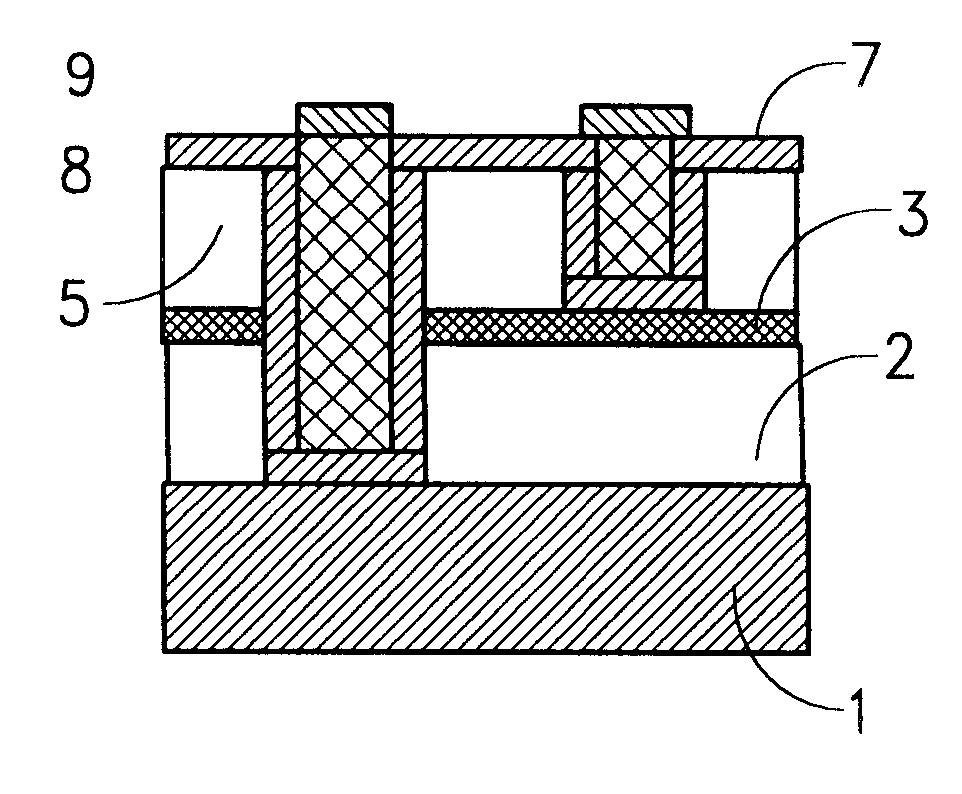
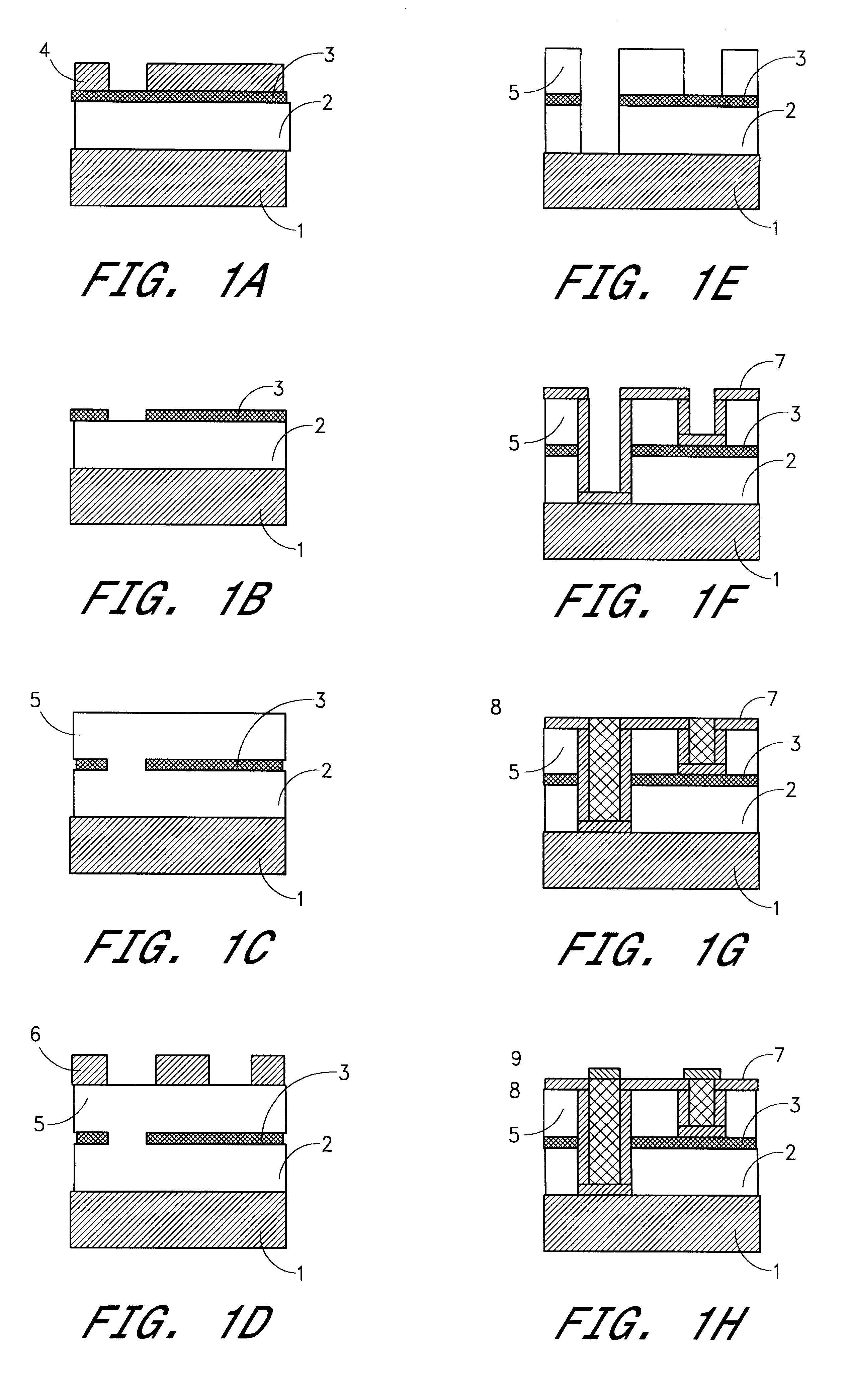
On a flattened substrate, i.e. a silicon wafer (1), a first fluorine-containing dielectric layer (2) is formed. This fluorine-containing dielectric can be a polymer like or ceramic like dielectric, e.g. a fluorinated silicon oxide. Alternatively this fluorine-containing dielectric can also be a dielectric where the fluorine is introduced only after the deposition, for instance by plasma fluorination. This holds for organic polymers comprising Phenyl groups. Examples of such polymers are the benzocyclobutarenes, i.e. benzocyclobutene (BCB) commercially available as Cyclotene 5021.TM., poly arylene ether, i.e FLARE.TM. II, aromatic hydrocarbon, i.e. SILK.TM., polyimides. An advantage of introducing fluorine after the deposition is that this fluorination can be performed locally.

A hard mask layer (3), e.g. a silicon nitride layer, is formed on the first fluorine-containing dielectric layer. A hard mask layer is defined as a layer which can be etched selective to the underlying dielectr...


PUM

PropertyMeasurementUnit
thicknessaaaaaaaaaa
thicknessaaaaaaaaaa
thicknessaaaaaaaaaa

Abstract

The present invention is related to a metallization structure on a fluorine-containing dielectric and a method for fabrication thereof. This metallization structure comprises a conductive pattern; a fluorine-containing dielectric; and a barrier layer containing a material, i.e. a near noble metal such as Co, Ni, Pt and Pd, said barrier layer comprising at least a first part, being positioned between said fluorine-containing dielectric and said conductive pattern, said first part containing at least a first and a second sub-layer, said first sub-layer contacting said fluorine-containing dielectric and being impermeable for fluorine. Particularly by depositing a layer of said material on a fluorine-containing dielectric, a stable and thin layer of a fluoride of said material is formed in a self-limiting way.

Description

The present invention is related to a new metallization structure being part of a structure used to interconnect electronic components or devices. Such components or devices can be part of an integrated circuit. Particularly, a multi-level Cu-containing metallization structure is disclosed based on fluorine-containing dielectrics.The ongoing miniaturization in integrated circuits with increased complexity and multilevel metal layers and the focus on increasing speed of these circuits demand for low permittivity materials, particularly for use as intermetal dielectric layers. Conventionally, metal interconnects, mostly aluminum layers, with silicon dioxide as intermetal dielectric are used, but this conventional solution will not be able to meet the stringent specifications resulting from the above mentioned trends. Therefore, to avoid that the larger portion of the total circuit delay is caused by the resistance and capacitance of the interconnect system, one has to reduce the permi...

Claims


Application Information

Patent Timeline
Patent Type & Authority Patents(United States)
IPC IPC(8): H01L23/532H01L23/52H01L23/522
CPCH01L23/5226H01L23/53223H01L23/53233H01L23/53238H01L23/5329H01L2924/0002
Inventor MAEX, KARENBAKLANOV, MIKHAIL RODIONOVICHVANHAELEMEERSCH, SERGE
Owner INTERUNIVERSITAIR MICRO ELECTRONICS CENT (IMEC VZW)
Why Eureka
Try Eureka