Microelectromechanical device manufacturing process

a manufacturing process and electromechanical technology, applied in the field of micro electromechanical systems (mems) devices, can solve the problems of significant environmental and manufacturing problems, significant volume of solvent is required to completely submerge the composite structure, and corrosive fumes are generated

Inactive Publication Date: 2002-01-08
TELEDYNE SCI & IMAGING
View PDF3 Cites 68 Cited by
  • Summary
  • Abstract
  • Description
  • Claims
  • Application Information

AI Technical Summary

Benefits of technology

During the dissolution step, an etchant is sprayed onto the composite structure from a plurality of nozzles. The nozzles are positioned to direct the etchant onto the composite structure at a rate sufficient to form a sheeting action on the composite structure. As active etchant is sprayed, spent acid is recovered either for subsequent re-use or for disposal. The progress of the etch process is observable through the windows of the tool since the etchant spray coats the composite structure with a transparent thin sheeting. The etch process is readily terminated since concentration of the etchant is more predictable than the immersion process described above. Advantageously, the present invention does not relay on a mixing action to remove spent solvent from the silicon wafer but rather encompasses a dynamic system where the solvent is constantly circulated. The improved method of the present invention the efficient utilization of the solvent minimizes the amount of solvent required to remove the inactive silicon material from the composite device.
The illustrated embodiment of the present invention provides improved throughput, improved repeatable and uniform etch rates, a reduction in the number of processing steps and chemical containment for improved safety compared to conventional dissolution processing techniques. Further, since the tool provides an enclosed chamber, escape of noxious fumes is significantly reduced.

Problems solved by technology

Unfortunately, the dissolution or dissolving of the substrate in the toxic solvent presents significant environmental and manufacturing problems.
For example, since the agitated solvent is heated to about 100.degree. C. toxic and corrosive fumes are generated.
Also, since the composite structure is fairly large, a significant volume of the solvent is required to completely submerge the composite structure.
Another problem with the solvent used in the dissolution method is that endpoint detection requires a visual analysis but visual detection is not possible while the composite structure is immersed because the EDP solvent, in large quantities, is highly opaque.
Further, characterizing the etch rate is difficult since the etch rate varies as a function of the concentration of the unspent solvent.
However, this is a noxious process that requires great care on the part of the operator and increases the probability of injury to the operator.
If the inspection is not performed very rapidly, the precipitates will render the device irreparably damaged and the entire wafer will have to be scrapped.
Although the risk of precipitate formation is reduced, the extended etch time often results in an over-etched MEMS device that will not function properly.
The residual contamination could render the device defective.
This immersion process subjects the operator to the risk of potential injury from scalding water if the composite structure is not carefully handled.
Often, the vacuum step is not successful, affecting device yields.
If there is significant delay in removal of the Dl water, the stiction force will permanently maintain the suspended portion in contact with the electrode rendering the MEMS device defective.
The above described dissolution process has poor yield due to poor process control, is very expensive and slow.
Further, the process is dangerous in that operators are exposed to toxic fumes and hot liquids.
While the above described process is acceptable for research and development or manufacturing small quantities of MEMS devices, scaling the process for large volumes is cost prohibitive.

Method used


Image

  • Microelectromechanical device manufacturing process
  • Microelectromechanical device manufacturing process
  • Microelectromechanical device manufacturing process

Examples


Embodiment Construction

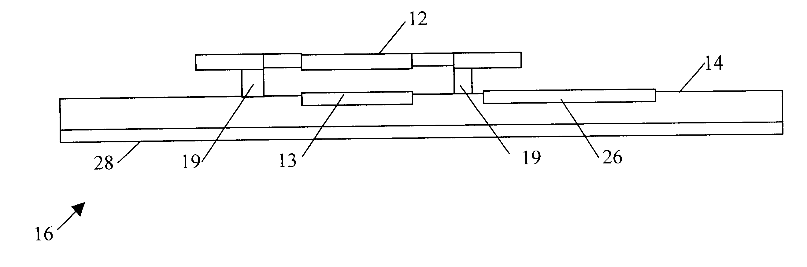
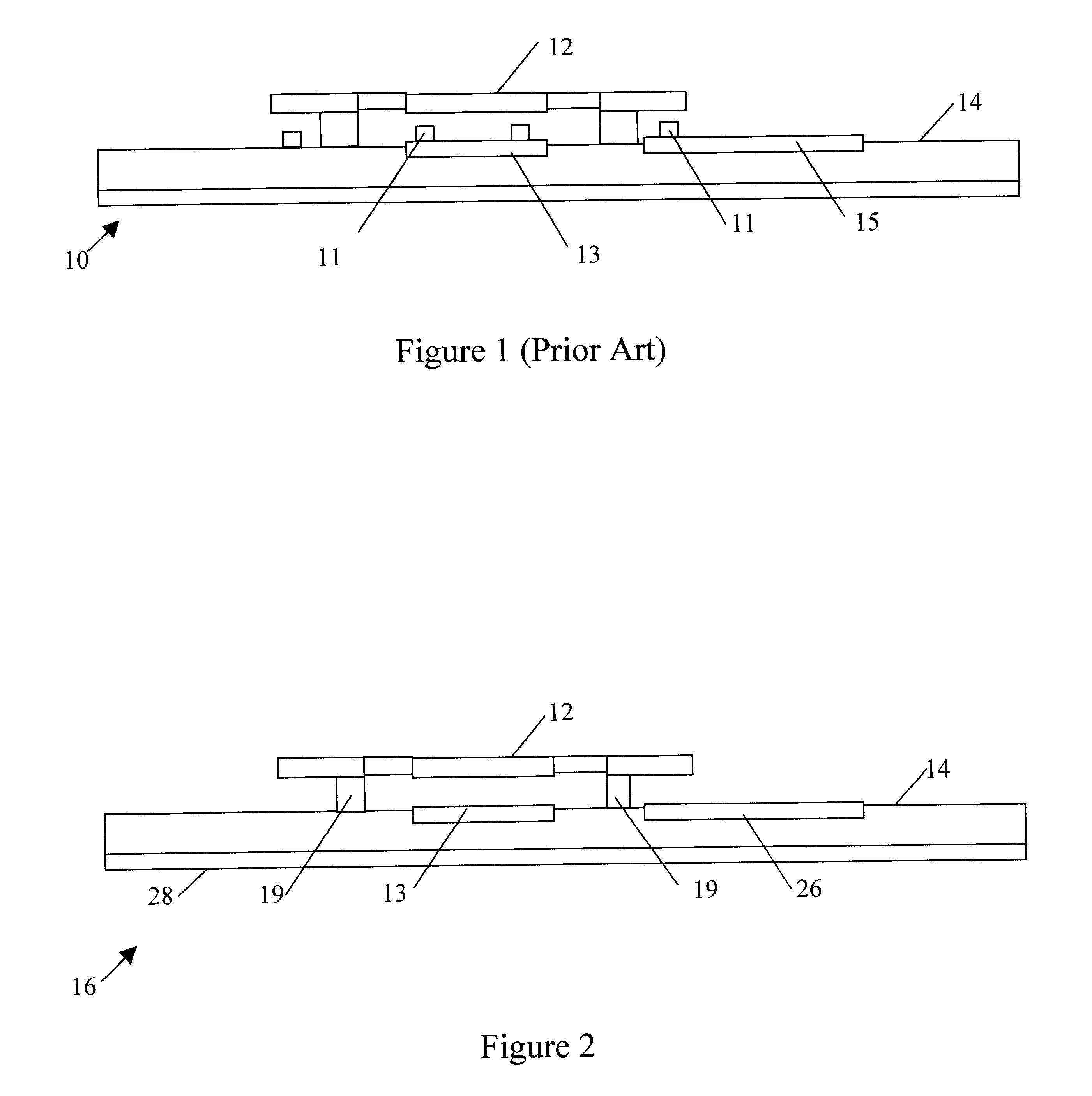
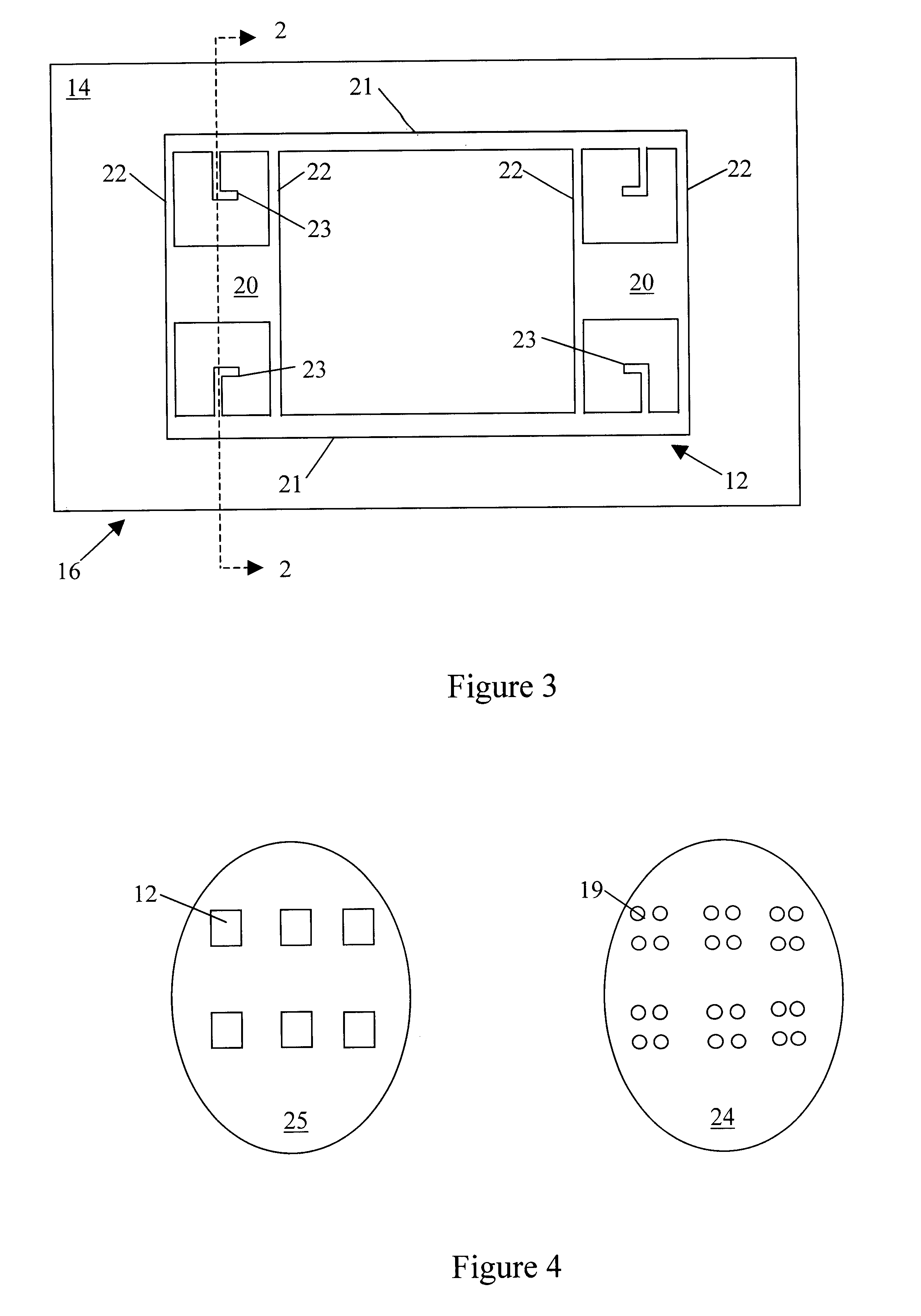
The present invention provides a method for manufacturing a MEMS device. In the following description, various MEMS devices are shown although it will be apparent to one of ordinary skill in the art that the present invention may be practiced without the specific structural or circuit details disclosed herein. In other instances, well known techniques or structural elements have not been shown in detail in order not to unnecessarily obscure the present invention. The present invention provides a method for the manufacture of MEMS devices with improved control of the manufacturing process. Advantageously, the present invention eliminates stiction forces that tend to cause MEMS structural elements to permanently adhere to the glass substrate as a result of the manufacturing process. The present invention also permits the efficient utilization of toxic etchant so as to minimize the risk posed to people and the environment.

A representative illustration of a prior art MEMS device 10 manu...


PUM

PropertyMeasurementUnit
thickaaaaaaaaaa
thicknessaaaaaaaaaa
opacityaaaaaaaaaa

Abstract

The present invention relates to micro electromechanical systems (MEMS) devices and more specifically to a process for manufacturing MEMS devices having at least one suspended structural element. The present invention seeks to provide an improved method for manufacture of MEMS devices having improved safety and increased yield and throughput compared to conventional EDP immersion process techniques. MEMS devices are made using a modified dissolution process that removes, in a selective etch step, inactive silicon to release an active silicon device from a sacrificial substrate. The present invention uses a selective etchant in conjunction with a commercial spray acid processing tool to provide a dissolution process with improved throughput, improved repeatable and uniform etch rates and reduction in the number of processing steps and chemical containment for improved safety. When the etch process is complete, the solvent spray is turned off and a spray of de-ionized water is directed onto composite structure to remove residual solvent without causing suspended elements to adhere to the support substrate.

Description

(1) Field of the InventionThe present invention relates to micro electromechanical systems (MEMS) devices and more particularly to a manufacturing process for manufacture of MEMS devices and application of such MEMS devices for a particular use.(2) Description of Related ArtMicro electromechanical MEMS devices are free-standing structural elements integrated on a substrate. MEMS devices are useful for many sensor or actuator applications such as electrical signal isolators, micro switches, or tuning fork gyroscopes, by way of example. A typical MEMS device has structural elements such as cantilevered beams, suspended platforms, capacitor plates, or other elements displaced from the supporting substrate. The size of these structural elements is typically on the order of millimeters.The manufacturing process for MEMS devices shares many of the same processing steps employed in the manufacture of integrated circuits, particularly patterning and etching steps. Unlike surface MEMS device...

Claims


Application Information

Patent Timeline
Patent Type & Authority Patents(United States)
IPC IPC(8): B81B3/00
CPCB81C1/00849B81C1/00928B81C2201/019B81C2201/0138
Inventor HUMPHREY, KURT D.
Owner TELEDYNE SCI & IMAGING
Why Eureka
Try Eureka