Method of forming silicon oxide layer and method of manufacturing thin film transistor thereby

Inactive Publication Date: 2002-01-08
LG DISPLAY CO LTD
View PDF16 Cites 53 Cited by
  • Summary
  • Abstract
  • Description
  • Claims
  • Application Information

AI Technical Summary

Benefits of technology

From the method of forming the silicon oxide layer, it improves the electric power consumption efficiency of the plasma CVD device and the formation speed of the layer. Fu

Problems solved by technology

As shown in the FIG. 13, however, the interspacing insulator is formed according to the step of the gate electrode or semiconductive layer, so that if the step coverage of the interspacing insulator is bad, there is a problem that the insulating pressure at the steps is lowered.
However, there are problems that the formation speed of the layer is slow, the insulating pressure is low, and so on, further it could not be used as the gate insulator.
Moreover, TEOS is in a liquid state at room temperature, so that it is difficult to employ the CVD using the TEOS after vaporizing this, and there is also the matter of high costs.
Regarding this silicon oxide layer, because the step coverage is too bad and there is a concern of generating cracks from the steps into the layer, it could be used to the gate insulator, but it is not suitable for the interspacing insulator.
However in this case, because of the process limitation according to the material gas, the degree of freedom in the process is

Method used


Image

  • Method of forming silicon oxide layer and method of manufacturing thin film transistor thereby
  • Method of forming silicon oxide layer and method of manufacturing thin film transistor thereby
  • Method of forming silicon oxide layer and method of manufacturing thin film transistor thereby

Examples


embodiment 1

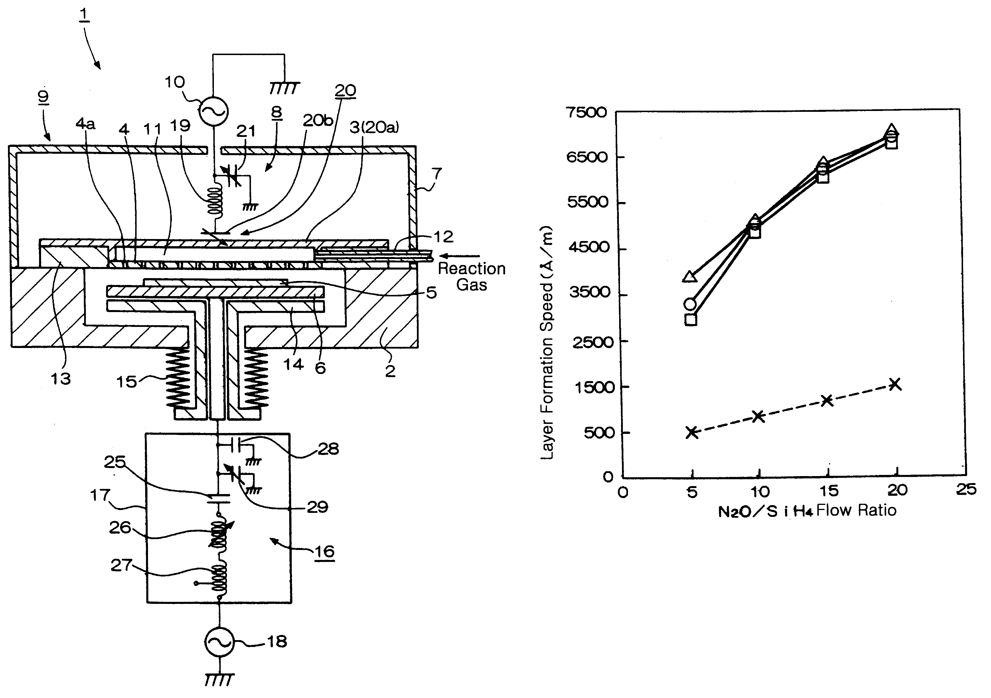
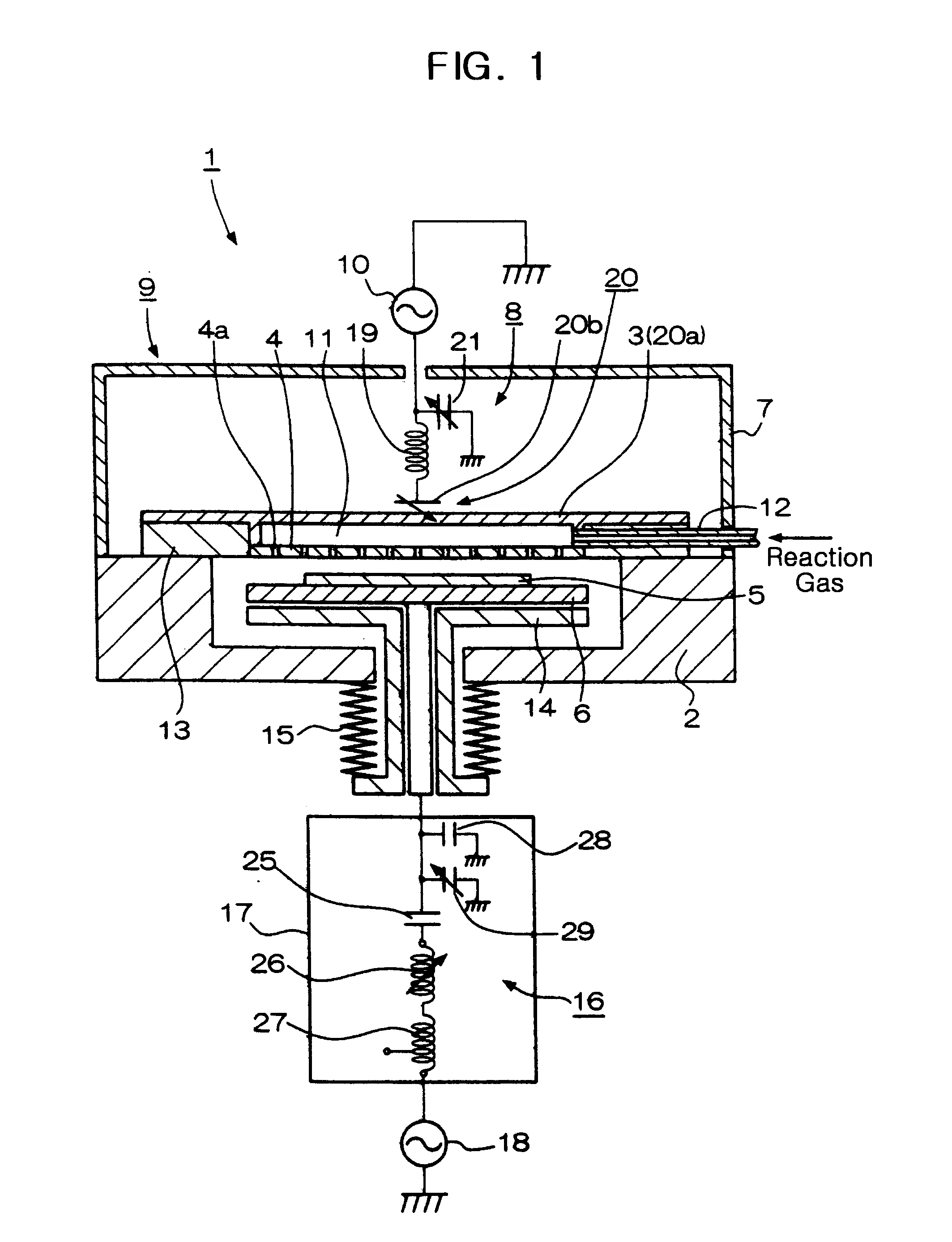
The present embodiment formed the silicon oxide layer by using the two frequency excitation plasma CVD device with the matching box described above.

FIG. 6 is a graph showing the relation of N.sub.2 O / SiH.sub.4 flow ratio versus the formation speed in variation of the substrate bias electric power rate(rf.sub.2) applied to the susceptor electrode when it used the two frequency excitation plasma CVD device of the above embodiment. The horizontal axis represents N.sub.2 O / SiH.sub.4 flow ratio, and the vertical axis represents the formation speed.

The formation condition of the layer was that the frequency of the high frequency electric power applied to the high frequency electrode was 13.56 MHz, the electric power (rf.sub.1) was fixed, the frequency of the substrate bias electric power applied to the susceptor electrode was 1.6 MHz, and the substrate bias electric power rate was 33.3% (this was represented as .quadrature. and solid line in the FIG. 6), 50% (this was represented as .smal...

embodiment 2

The variation of the insulating pressure of the formed silicon oxide layer was investigated according to the applied of the substrate bias electric power.

FIG. 7 is a graph showing the relation of the substrate bias electric power rate versus the insulating pressure of the silicon oxide layer with using the present two frequency excitation plasma CVD device. The horizontal axis represents the substrate bias electric power rate (%), and the vertical axis represents the insulating pressure(MV / cm).

The formation condition of the layer was that the frequency of the high frequency electric power applied to the high frequency electrode was 40.68 MHz, the high frequency electric power rf.sub.2 was fixed, the frequency of the substrate bias electric power applied to the susceptor electrode was 1.6 MHz, the substrate bias electric power rate was 0%, 14.3%, 40%. And, the temperature of the substrate was 300.degree. C., the pressure in the chamber is 200 Pa.

As to the reaction gas, the N.sub.2 O / ...

embodiment 3

In the present method of forming the silicon oxide layer, the changes of the characteristics of the formed silicon oxide layer were investigated according to the variation of the N.sub.2 O / SiH.sub.4 flow ratio.

FIG. 9 is a graph showing the relation of N.sub.2 O / SiH.sub.4 flow ratio versus the formation speed of the silicon oxide layer with using the two frequency excitation plasma CVD device. At this time, SiH.sub.4 flow ratio occupied in the reaction gas was 1% (this was represented as .quadrature. and solid line in the FIG. 9), 2% (this was represented as .smallcircle. and solid line in the FIG. 9), 3% (this was represented as .DELTA. and solid line in the FIG. 9).

In FIG. 9, the horizontal axis represents the N.sub.2 O / SiH.sub.4 flow ratio, and the vertical axis represents the formation speed of the layer in .ANG. / min.

The formation condition of the layer was that the frequency of the high frequency electric power applied to the high frequency electrode was 40.68 MHz, the frequency...


PUM

PropertyMeasurementUnit
Fractionaaaaaaaaaa
Fractionaaaaaaaaaa
Fractionaaaaaaaaaa

Abstract

The present method of forming a silicon oxide layer comprises providing two frequency excitation plasma CVD device which comprises a high frequency electrode, a susceptor electrode, and two matching box for impedance matching between the electrodes and a power supply, wherein one side electrode constituting a tuning condenser of a matching box toward the high frequency electrode is the high frequency electrode; placing a substrate on the susceptor electrode; applying high frequency electric power on the high frequency electrode and the susceptor electrode respectively; and forming a silicon oxide layer on the substrate by generating plasma with using a reaction gas of which main reaction gas is a mixing gas of monosilane and nitrous oxide.

Description

This application claims the benefit of Japanese Patent Application No. 1998-309237, filed on Oct. 29, 1998, which is hereby incorporated by reference.1. Field of the InventionThe present invention relates to a method of forming silicon oxide layer and method of manufacturing thin film transistor (TFT) thereby, and more particularly, to a method of forming silicon oxide layer preferably used as a gate insulator and an interspacing insulator.2. Discussion of the Related ArtA liquid crystal display device (LCD) has been used widely to be minimized, lightened, and thinned, for example, an active matrix LCD of a twisted nematic (TN) mode has been known as a display device which has a low driving voltage, a small electric power consumption, a high contrast, and a high image quality.In the active matrix LCD, a pair of substrates are opposing each other by interposing a liquid crystal layer, and one substrate between them is an active matrix substrate which has a switching element driving a...

Claims


Application Information

Patent Timeline
IPC IPC(8): C23C16/40C23C16/509C23C16/50H01L21/02H01J37/32H01L21/316H01L21/336H01L21/31H01L29/786
CPCC23C16/402C23C16/5096H01J37/32082H01J37/32165H01J37/32183H01L21/02211H01L21/02274H01L21/31612H01L21/02164Y10S438/931H01L29/66757H01L29/786
Inventor KIM, KWANG NAMCHAE, GEE SUNG
Owner LG DISPLAY CO LTD
Why Eureka
Try Eureka