
Method for manufacturing semiconductor devices

a manufacturing method and semiconductor technology, applied in semiconductor devices, semiconductor/solid-state device details, electrical devices, etc., can solve the problems of reducing production yield, deteriorating resistance to electromigration, and requiring a high barrier capability

Inactive Publication Date: 2002-02-26
SEIKO EPSON CORP
View PDF12 Cites 43 Cited by
  • Summary
  • Abstract
  • Description
  • Claims
  • Application Information

AI Technical Summary

Benefits of technology

In accordance with a preferred embodiment, a metal layer for a barrier layer is formed first by a sputtering method or a CVD method, and then, the metal layer is subjected to a heat treatment in a nitrogen atmosphere to form a metal nitride layer. As a result, the metal nitride film is formed with a higher cohesiveness with a better coverage at the bottom area of the through hole compared to a metal nitride film that is directly grown by sputtering a metal nitride. Moreover, a barrier layer formed by the process described above has a greatly improved barrier capability, mainly because the metal nitride layer in the barrier layer is densified and the metal oxide layer is formed in the barrier layer.

Problems solved by technology

However, such a contact structure tends to result in greater electrical resistance of the tungsten, deterioration of resistance to electromigration and lowered production yield due to its complicated forming process.
However, contact sections that use aluminum require complete countermeasures against junction leak that may be caused by reaction between the aluminum and silicon of the silicon substrate and also require a high barrier capability of a barrier layer.
1 A titanium nitride layer, when formed by reactive sputtering in a nitrogen atmosphere, has an insufficient coverage.
Therefore, the formed titanium nitride layer does not provide a sufficient coverage at a bottom portion of a miniaturized through hole that has a high aspect ratio.
2 A titanium nitride layer, when formed by reactive sputtering in a nitrogen atmosphere, has large stresses and therefore tends to develop microscopic cracks.
As a result, aluminum in the wiring material tends to diffuse and cause junction leaks.
As a result, aluminum tends to diffuse through crystal grain boundaries and cause junction leaks.
As a result, the surface of the aluminum layer roughens and mask alignment becomes difficult.
5 Further, a titanium nitride layer, when formed by reactive sputtering in a nitrogen atmosphere, occasionally peels off during film growth because of its own film stresses and therefore tends to generate particles.
The particles pollute the surface of the wafer and cause short-circuits, which results in a lowered production yield.

Method used


Image

  • Method for manufacturing semiconductor devices
  • Method for manufacturing semiconductor devices
  • Method for manufacturing semiconductor devices

Examples


Embodiment Construction

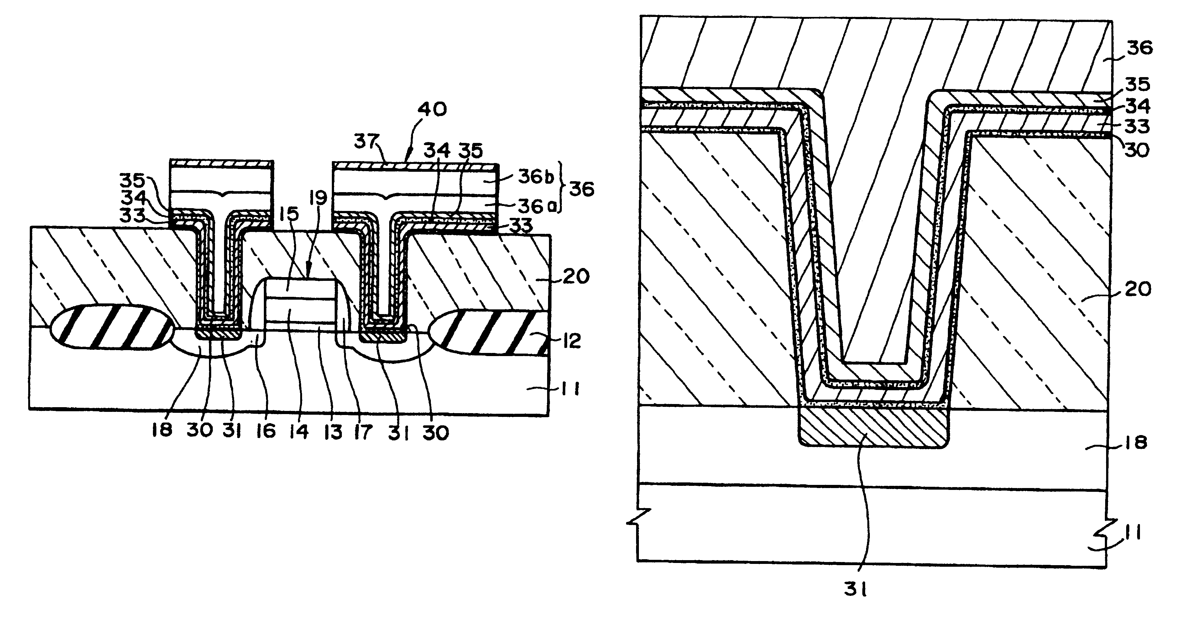
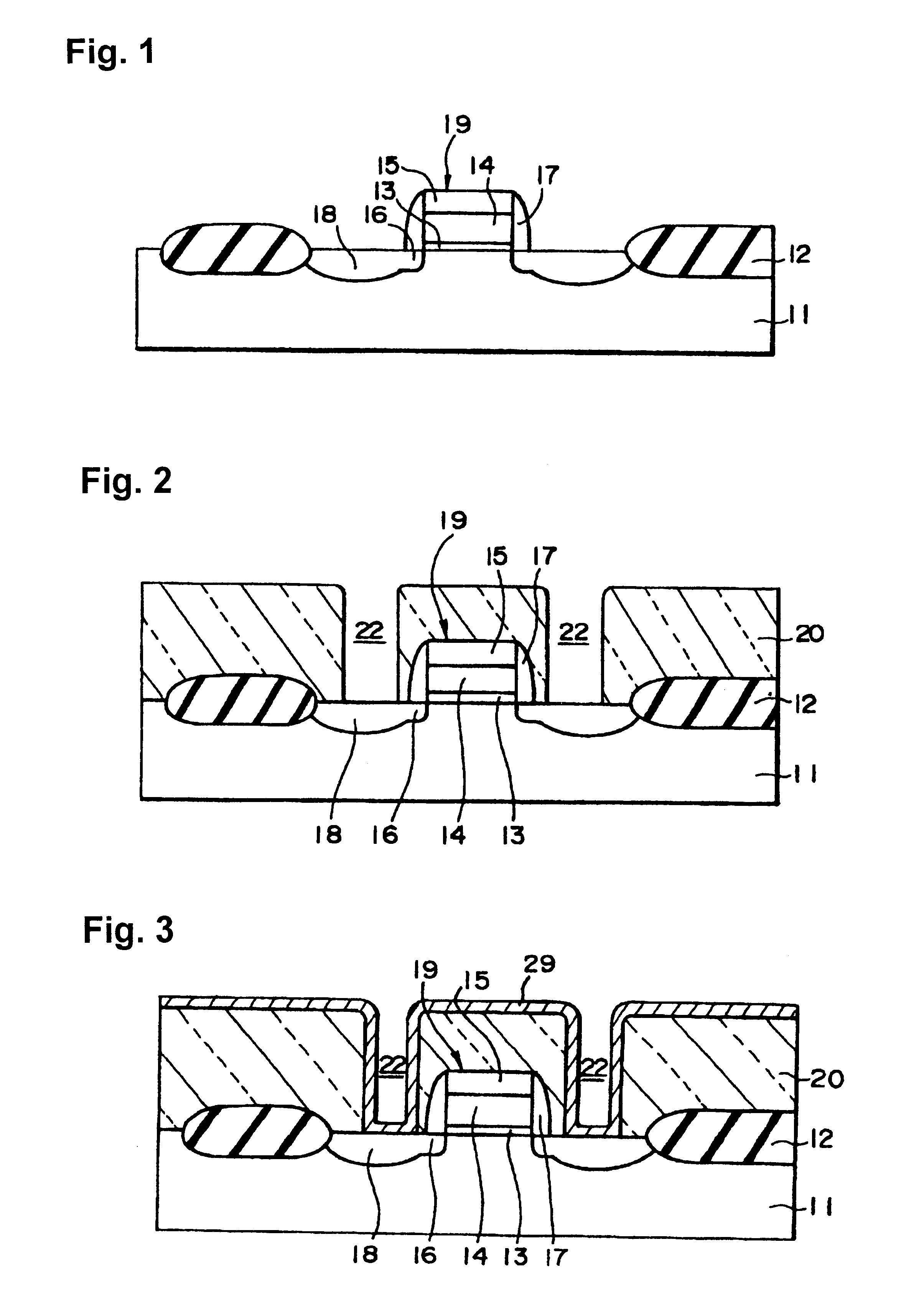
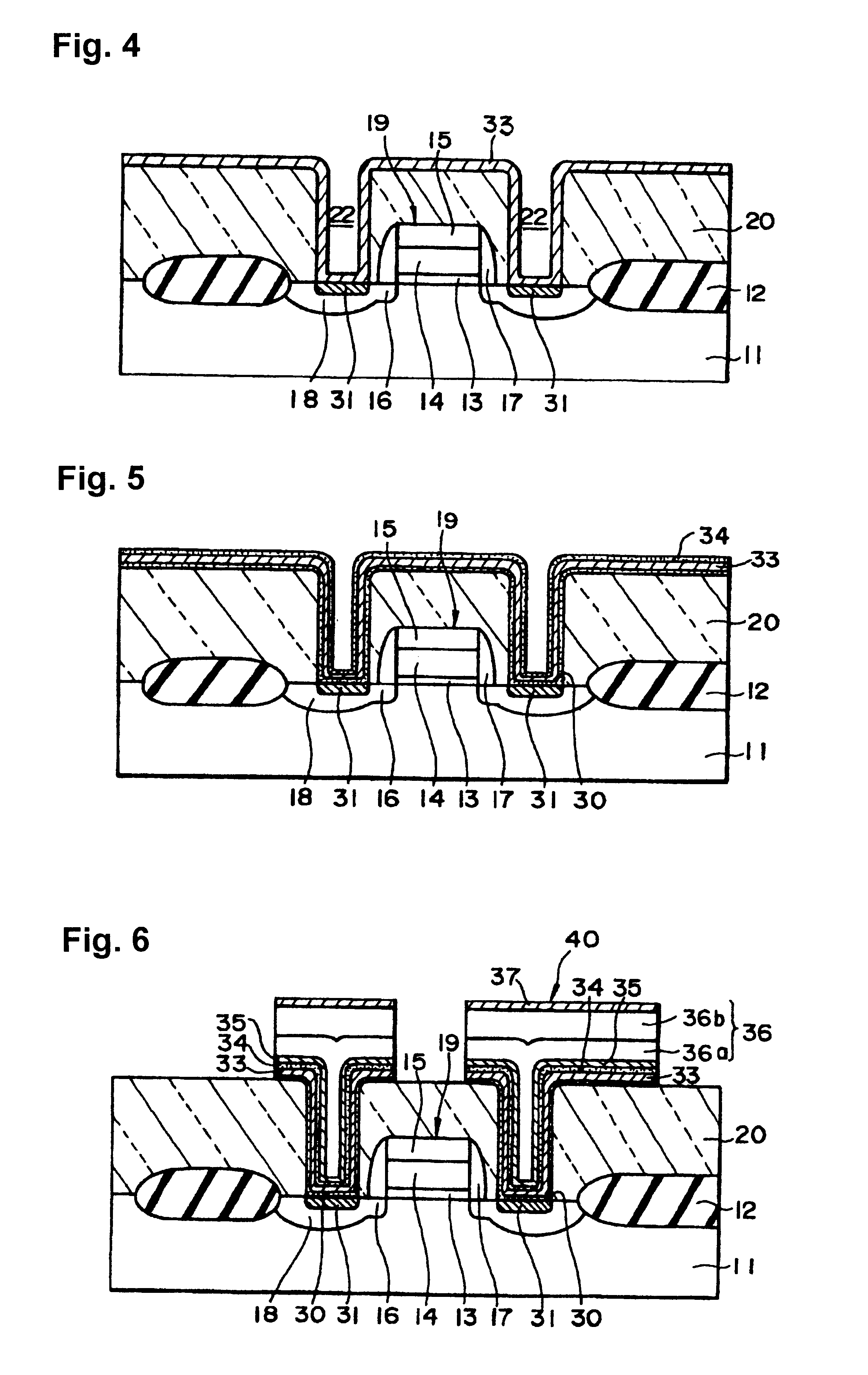
Referring to FIGS. 1-6, a method of manufacturing a semiconductor device will be described. FIG. 7 schematically shows a cross-sectional view of a semiconductor device manufactured by a method in accordance with one embodiment of the present invention.

A MOS device is formed in a silicon substrate 11 by a commonly practiced method, as shown in FIG. 1. More specifically, for example, a field insulation layer 12 is formed on the silicon substrate 11 by selective oxidation, and a gate oxide layer 13 is formed in an active region. A threshold voltage level is adjusted by channel injection. Then a polysilicon layer 14 is grown on the gate oxide layer 13 by thermally decomposing monosilane (SiH.sub.4), and a tungsten silicide layer 15 is sputter-deposited on the polysilicon layer 14. Further, the layers are etched to a specified pattern to form a gate electrode 19.

Then, phosphorous is ion-implanted to form a low concentration impurity layer 16 for a source region or a drain region. Side-wa...


PUM


Abstract

A semiconductor device is manufactured by a method including the steps of forming a through hole in an interlayer dielectric layer (silicon oxide layer, BPSG layer, etc.) formed on a semiconductor substrate having a device element. A barrier layer is formed on surfaces of the interlayer dielectric layer and the through hole. A wiring layer is formed on the barrier layer. The barrier layer is formed by a method including the following steps. A titanium layer that forms at least a part of the barrier layer is formed. A heat treatment is conducted in a nitrogen atmosphere to form a titanium nitride layer at least on a surface of the titanium layer. The titanium nitride layer is contacted with oxygen in an atmosphere including oxygen. A heat treatment is conducted in a nitrogen atmosphere to form titanium oxide layers and to densify the titanium nitride layer.

Description

1. Field of the InventionThe present invention relates to a method for manufacturing semiconductor devices and, more particularly, to a method for manufacturing the semiconductor device that has an excellent barrier capability in a miniaturized contact section of the semiconductor device.2. Description of Related ArtWith higher device miniaturization, higher density integration and increased multiple layers of LSI devices, it has become an important subject to develop techniques for embedding wiring material in miniaturized through holes with greater aspect ratios. In the conventional technique, for example, a tungsten plug is embedded in a through hole in a contact section having an aperture diameter of 0.5 .mu.m or smaller and an aspect ratio of 2 or greater. The tungsten plug is required in order to plug the through hole and to prevent reaction between aluminum of the wiring layer and silicon of the silicon substrate. However, such a contact structure tends to result in greater e...

Claims


Application Information

Patent Timeline
IPC IPC(8): H01L21/70H01L21/768H01L21/28H01L21/336H01L21/3205H01L23/52H01L29/78
CPCH01L21/76843H01L21/76846H01L21/76888H01L21/76864H01L21/76856
Inventor ASAHINA, MICHIOSUZUKI, EIJIMATSUMOTO, KAZUKIMORIYA, NAOHIRO
Owner SEIKO EPSON CORP
Learn More