Advanced thermal gradient DNA chip (ATGC), the substrate for ATGC, method for manufacturing for ATGC, method and apparatus for biochemical reaction, and storage medium

a technology of thermal gradient and dna chip, which is applied in the field of advanced thermal gradient dna chip, which can solve the problems of reducing the amount of formation, the inability of single stranded polynucleotide to effectively bond with a probe, and the decline of measuring resolution

Inactive Publication Date: 2002-08-06
HITACHI LTD
View PDF3 Cites 20 Cited by
  • Summary
  • Abstract
  • Description
  • Claims
  • Application Information

AI Technical Summary

Problems solved by technology

When a temperature is higher than Tm, a single stranded polynucleotide is hard to bond effectively with a probe.
On the other hand, when a temperature is lower than Tm, the background noise resulting from the mismatch bonding increases, leading to the decline of measuring resolution.
Thus, in a case where different kinds of probes are immobilized on the polynucleotide detection chip, when the probes are hybridized with the single stranded polynucleotide sample while keeping the temperature constant on the chip, this gives rise to problems such as differences in the amount of the formation of hybridization and differences in mismatching probability occurring due to the difference in thermal stability among individual probes.
Such an attempt, however, is not sufficient for fully eliminating the effect of the difference in Tm.
However, this method frequently results in the probe binding with a substance other the subject that to be detected, causing the noise in detecting the subject.
When the reaction is allowed to proceed at the melting temperature only by heating the reaction system, the oligonucleotide probe may bind with a nucleotide other than the nucleotide having the complementary strand to the probe (the subject of detection), resulting in so-called mismatching that causes the noise in detecting the subject.

Method used


Image

  • Advanced thermal gradient DNA chip (ATGC), the substrate for ATGC, method for manufacturing for ATGC, method and apparatus for biochemical reaction, and storage medium
  • Advanced thermal gradient DNA chip (ATGC), the substrate for ATGC, method for manufacturing for ATGC, method and apparatus for biochemical reaction, and storage medium
  • Advanced thermal gradient DNA chip (ATGC), the substrate for ATGC, method for manufacturing for ATGC, method and apparatus for biochemical reaction, and storage medium

Examples


example 2

Chip Manufacturing Process

Referring to FIG. 7 through FIG. 9, the manufacturing process of the DNA chip substrate, on which the islands are formed in the mesh structure on a composite membrane of SiO.sub.2 and SiN, will be described.

FIG. 7 is a diagram illustrating the first manufacturing process of the DNA chip substrate. In this embodiment, an n-type Si substrate (N-sub) 71, having plane (100) as a surface area and thickness of 500 .mu.m, is used as a substrate. After forming p-well pattern with the SiO.sub.2 membrane 74 on the surface of the substrate, p-wells (1018 pieces / cm.sup.3) 72 and 73, having a depth of 3 .mu.m, respectively, are formed by B doping and diffusion, in order to electrically insulate the temperature detection element 6 to be formed later by n+ diffusion and heater circuit 5. An SiO.sub.2 membrane 74 is formed as a mask for separating elements and for diffusion. A dope such as boric acid is used for the p-well diffusion. Then, after forming a circuit pattern w...

example 3

Probe Immobilizing Process

The process for immobilizing oligonucleotide probes on a manufactured chip will be described in the following. First, OH group is introduced to the silicon nitride membrane on the surface of a chip. For this purpose, in general, the hydrolytic method by using the mixture of H.sub.2 SO.sub.4 and H.sub.2 O.sub.2, the mixture of NaOH and H.sub.2 O.sub.2 and the like is employed. Further, the method in which the chip is simply left immersed in water for a certain period time is also applicable.

Next, a silane coupling agent such as the epoxy resin and the like is injected onto the surface of a chip to silanize the silicon nitride membrane. In this process, the previously introduced OH group combines with the silane coupling agent. In this embodiment, 3-glycidoxypropiltrimethoxy silane is used as a silane coupling agent. The reaction is carried out at room temperature for 30 minutes and followed by baking at 120.degree. C. for 1 hour are given.

Next, oligonucleoti...

example 4

Temperature Control

The apparatus for controlling the DNA chip will be described in the following.

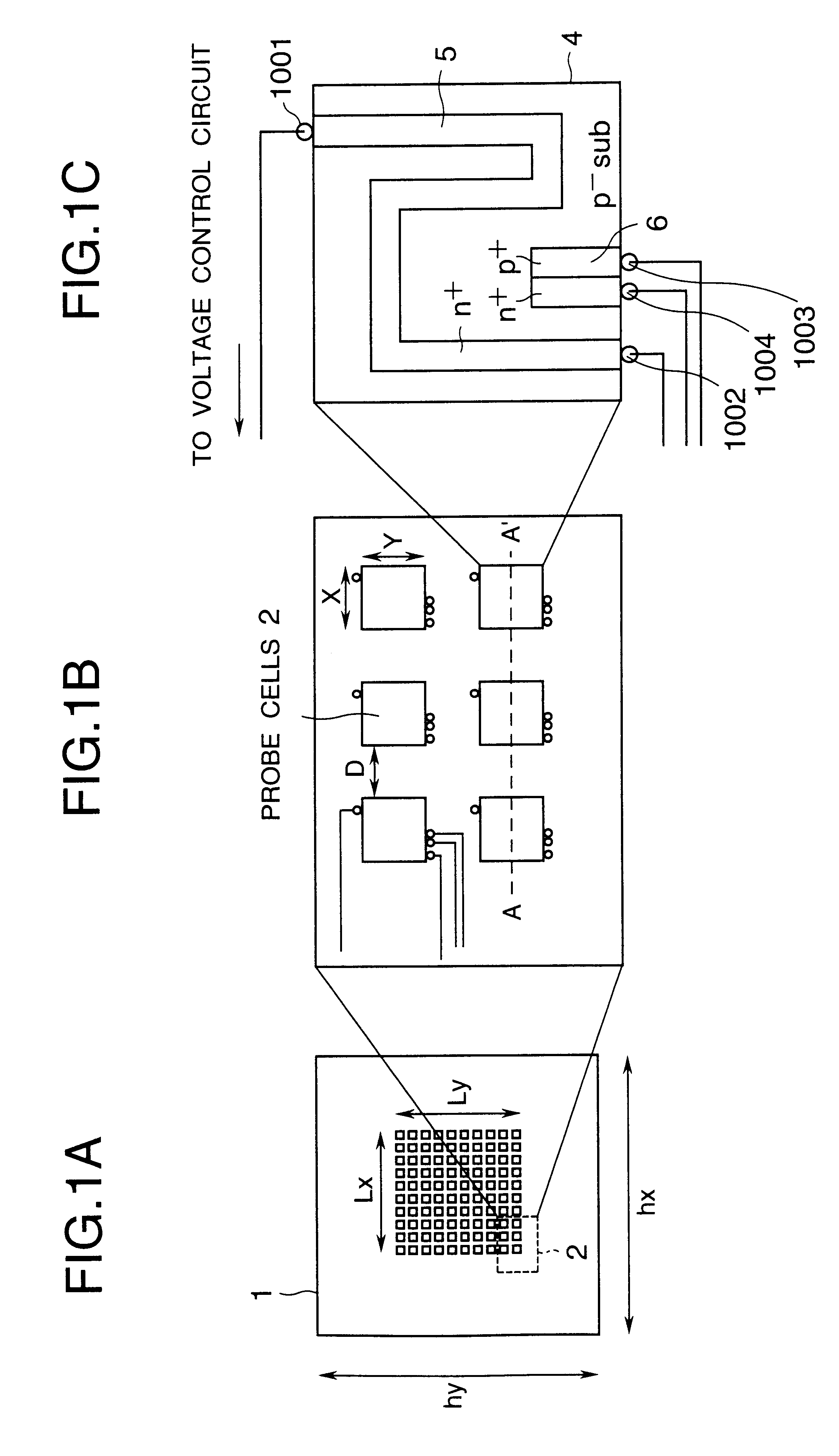
FIG. 10 is a diagram illustrating an example of the biochemical reaction detection apparatus. DNA chip 101 comprises probe cells, each provided with a heater terminal (+) 1001, a heater terminal (-) 1002, a temperature detection terminal (+) 1003 and a temperature detection terminal (-) 1004, and wiring for these terminals and controller 105 is similar to that shown in FIG. 18. The controller 105 comprises a temperature detection circuit 182, including a voltmeter 110, a power source Vc and a resistance R, and a heater power source circuit 181, including a heater power source Vpo, an output controller 111 and a switch 109, both of which are equivalent in number to the number of probe cells to be temperature-controlled independently from one another. FIG. 18 shows only one set of such components. Wirings to these terminals are connected to a holder 103 through a printed circuit board 102,...


PUM

PropertyMeasurementUnit
Tmaaaaaaaaaa
Tmaaaaaaaaaa
Tmaaaaaaaaaa

Abstract

A biochemical reaction detection chip capable of controlling the temperature for biochemical reactions including hybridizations and its substrate. The function of the chip is performed by comprising a plurality of islands of a heat conducting material on the membrane of the substrate, the islands being spaced from each other and individually provided with temperature controllers, and the probes immobilized on the substrate.

Description

The present invention relates to an advanced thermal gradient DNA chip (ATGC), a substrate for ATGC, a method of manufacturing of ATGC, a method and an apparatus for biochemical reaction and a storage medium.DESCRIPTION OF THE RELATED ARTAs a method for determining a base sequence of a nucleic acid, the method for detecting hybridization between a single stranded polynucleotide of interest and a single stranded oligonucleotide probe previously designed, by using the polynucleotide detection chip with the single stranded oligonucleotide probes immobilized on its different areas depending on the type of sequences,are known. Examples of the polynucleotide detection chips include polynucleotide detection chips for diagnosis, where DNAs complementary to specific mutated sequences of interest are arranged (Science, Vol. 270, 467-470, 1995) and those for SBH (Sequencing By Hybridization) method, in which the oligonucleotide probes capable of hybridizing with all the possible base sequences...

Claims


Application Information

Patent Timeline
Patent Type & Authority Patents(United States)
IPC IPC(8): B01L7/00B01J19/00C12Q1/68B01L3/00C12Q1/6837C40B40/06C40B60/14
CPCB01J19/0046B01L7/52B01L7/54C12Q1/6837B01J2219/00495B01J2219/00497B01J2219/00527B01J2219/00529B01J2219/00585B01J2219/00596B01J2219/00605B01J2219/00608B01J2219/00612B01J2219/00626B01J2219/00637B01J2219/00659B01J2219/00689B01J2219/00695B01J2219/00707B01J2219/00722B01L3/50851B01L2300/0636B01L2300/0819C40B40/06C40B60/14C12Q2527/107Y10S977/924
Inventor KAJIYAMA, TOMOHARUMIYAHARA, YUJIMURAKAWA, KATSUJI
Owner HITACHI LTD
Why Eureka
Try Eureka