

Nitride semiconductor device and method of manufacturing the same
a semiconductor device and nitride technology, applied in the direction of polycrystalline material growth, crystal growth process, chemically reactive gas, etc., can solve the problems of restricting the kind of substrate to be used, affecting the growth of crystals of good quality usable for semiconductor devices, and difficult growth under conditions
- Summary
- Abstract
- Description
- Claims
- Application Information
AI Technical Summary
Problems solved by technology
Method used
Image

Examples
example 1
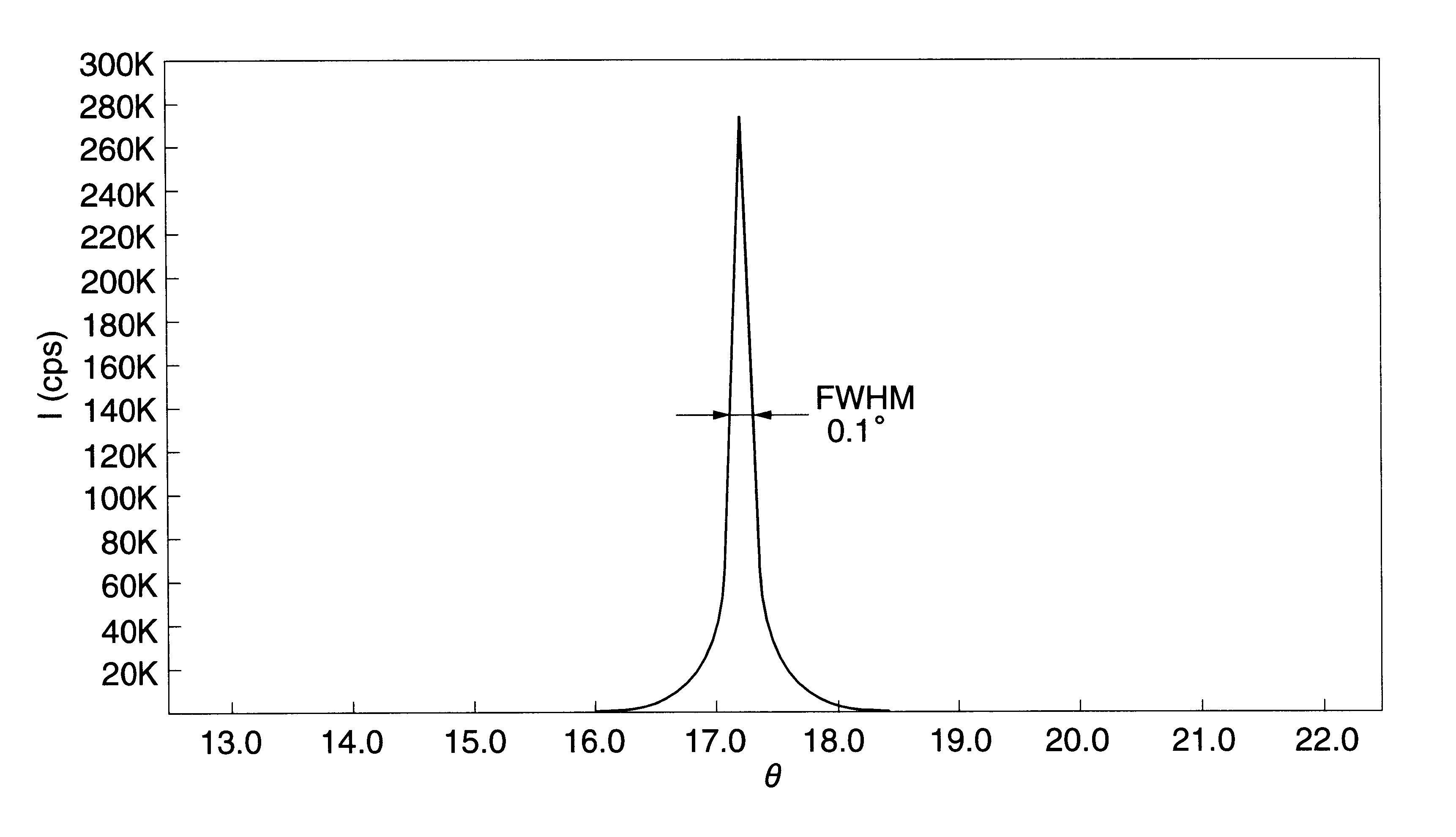
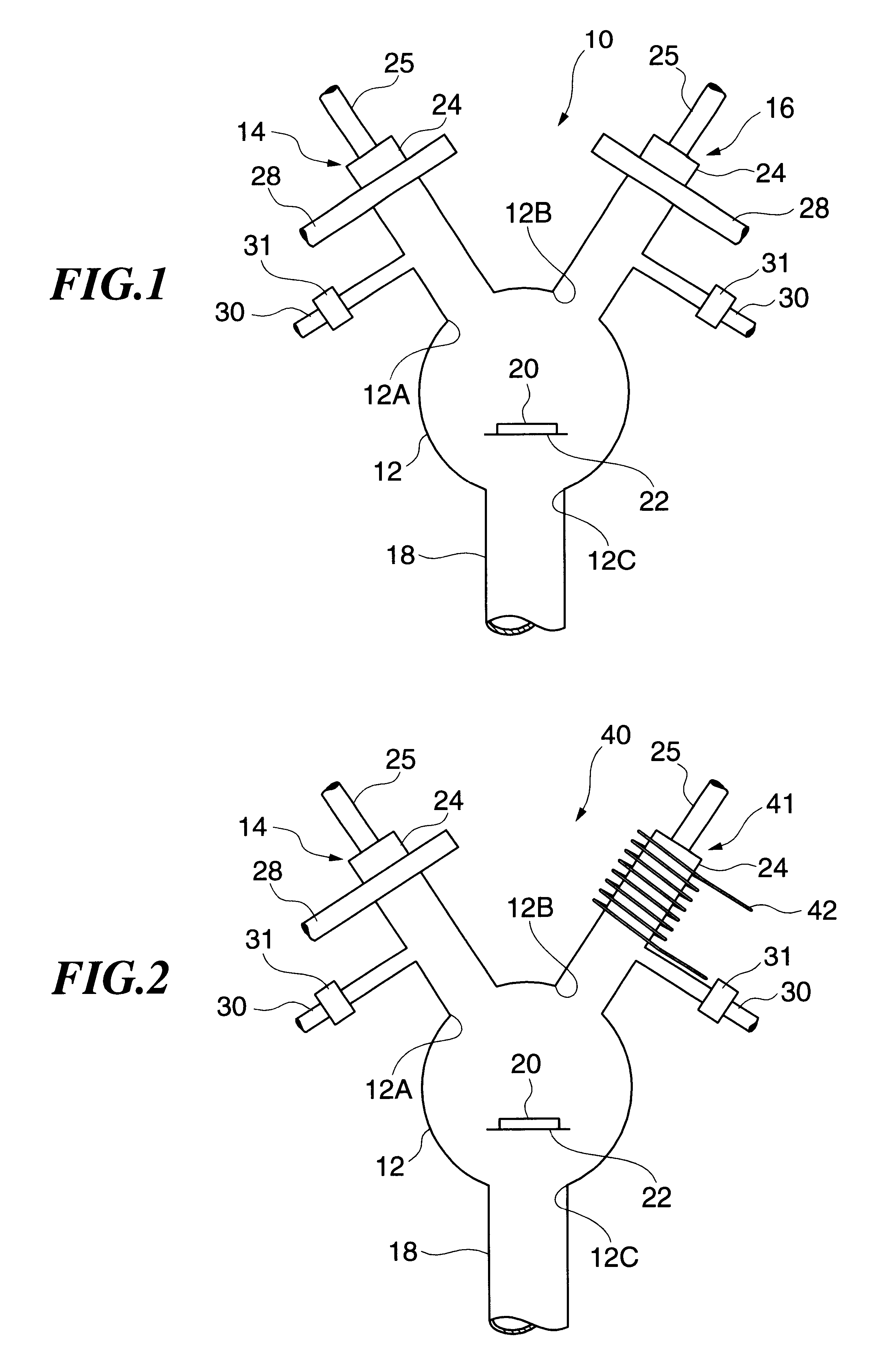
A nitride semiconductor device was manufactured by using the semiconductor device manufacturing apparatus 10 shown in FIG. 1. That is, a sapphire substrate with (0001) face was set to the substrate holder 20, the substrate temperature was controlled to 380.degree. C. by the substrate heater 22, and nitrogen was introduced from the gas supplying tube 25 of the first starting material activating-supplying portion 14 at a flow rate of 2 L / min into the reactor 12. The pressure inside the reactor 12 was controlled to 45 Pa. A nitrogen gas passing through the microwave guide tube 28 of the first starting material activating-supplying portion 14 was plasma-discharged by a microwave at 2.45 GHz. The microwave power in this case was set to 400 W.
Then, trimethyl gallium was introduced as it was from the gas introducing tube 30 of the first starting material activating-supplying portion 14 into the reactor 12 to grow gallium nitride directly on the sapphire substrate. Trimethyl gallium describ...
example 2
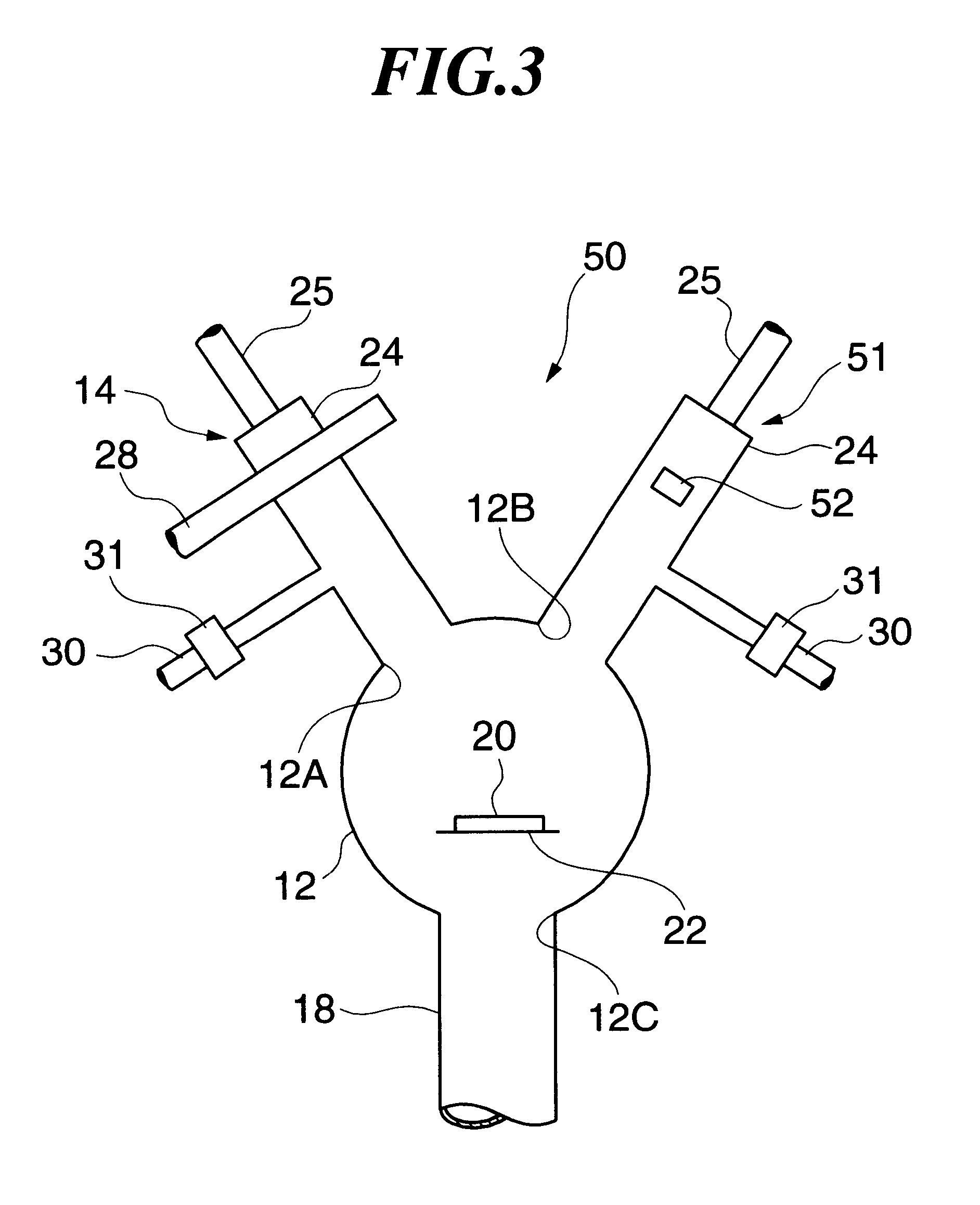
A nitride semiconductor device was manufactured by using the semiconductor device manufacturing apparatus 50 shown in FIG. 3. That is, a sapphire substrate with (0001) face was set to the substrate holder 20, the substrate temperature was controlled to 380.degree. C. by the substrate heater 22, and nitrogen was introduced at a flow rate of 2 L / min from the gas supplying tube 25 of the first starting material activating-supplying portion 14 into the reactor 12. The nitrogen gas passing through the microwave guide tube 28 of the first starting material activating-supplying portion 14 was plasma-discharged by a microwave at 2.45 HGz. In this case, the microwave power was set to 400 W. Further, nitrogen was introduced at a flow rate of 1 L / min from the gas introducing tube 25 of the second starting material activating-supplying portion 51 into the reactor 12. The nitrogen gas was caused to discharge by the high frequency at 13.56 MHz. In this case, rf power was set to 100 W. The pressur...
PUM
| Property | Measurement | Unit |
|---|---|---|
| temperature | aaaaa | aaaaa |
| temperature | aaaaa | aaaaa |
| temperature | aaaaa | aaaaa |
Abstract
Description
Claims
Application Information