Method of etching tungsten or tungsten nitride electrode gates in semiconductor structures

Inactive Publication Date: 2002-08-27
APPLIED MATERIALS INC
View PDF12 Cites 28 Cited by
  • Summary
  • Abstract
  • Description
  • Claims
  • Application Information

AI Technical Summary

Problems solved by technology

In particular, when the O.sub.2 concentration is greater than about 20% by volume in the plasma source gas, further increases in O.sub.2 content have a limite

Method used


Image

  • Method of etching tungsten or tungsten nitride electrode gates in semiconductor structures
  • Method of etching tungsten or tungsten nitride electrode gates in semiconductor structures
  • Method of etching tungsten or tungsten nitride electrode gates in semiconductor structures

Examples


Embodiment Construction

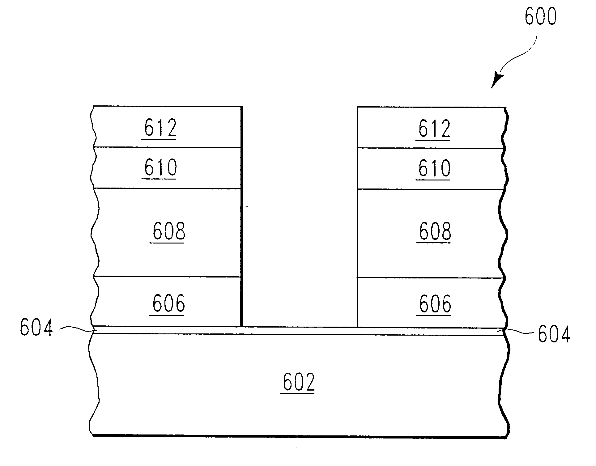
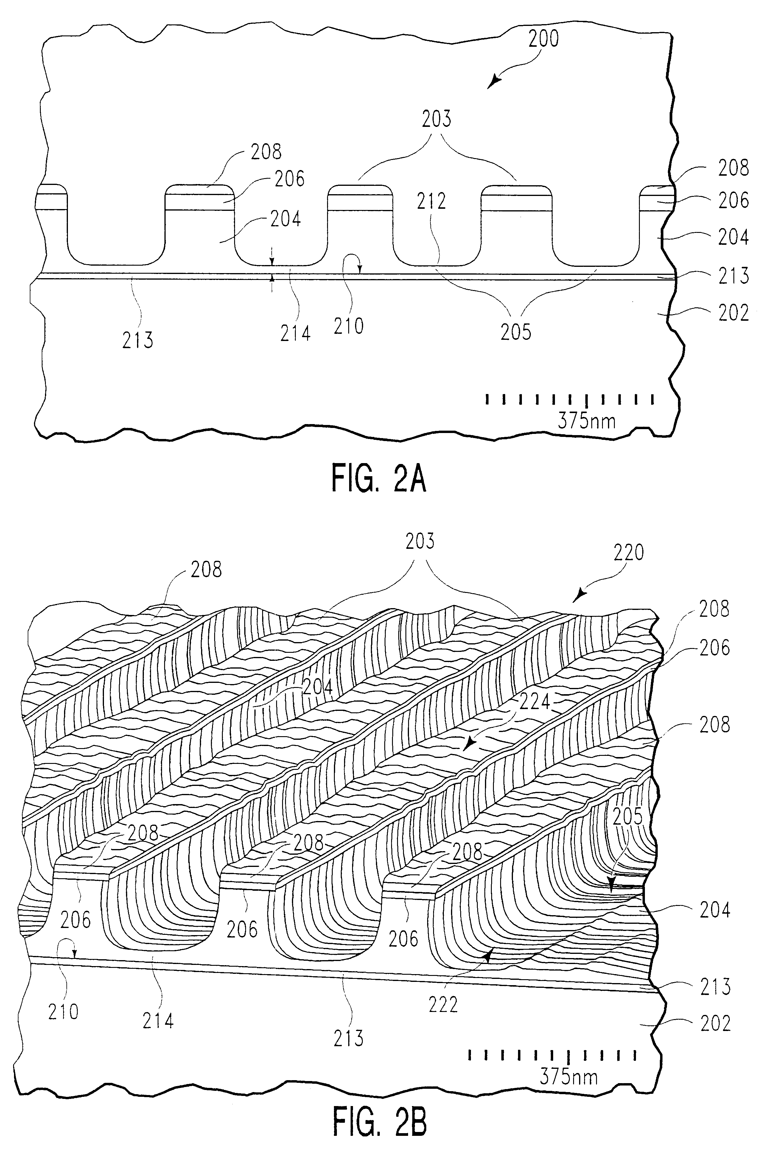
FIG. 2A shows a cross-sectional side view schematic of an etched tungsten structure 200, where the etched pattern is lines 203 and spaces 205. The line width is approximately 0.165 .mu.m, and the space width is approximately 0.21 .mu.m. The structure includes a thin (.apprxeq.45 .ANG.) silicon oxide layer 213 on a silicon substrate 202, overlying silicon oxide layer 213 is a 1650 .ANG. thick layer of tungsten 204, a 400 .ANG. thick image-focusing antireflective coating (ARC) layer 206, and the residue 208 of a photoresist layer which was used to pattern the etched structure 200. The tungsten layer 204 includes a thin (.about.100 .ANG.) wetting layer of tungsten nitride (not shown) which aids in adhesion of the tungsten to the silicon oxide layer 213. The tungsten nitride is etched during the same etch process as the tungsten. Therefore, as used herein, the term "tungsten layer" refers to a layer of tungsten, optionally in combination with a thin underlying layer of tungsten nitride....


PUM

PropertyMeasurementUnit
Fractionaaaaaaaaaa
Fractionaaaaaaaaaa
Fractionaaaaaaaaaa

Abstract

The present invention relates to a method of etching tungsten or tungsten nitride in semiconductor structures, and particularly to the etching of gate electrodes which require precise control over the etching process. We have discovered a method of etching tungsten or tungsten nitride which permits precise etch profile control while providing excellent selectivity, of at least 175:1, for example, in favor of etching tungsten or tungsten nitride rather than an adjacent oxide layer. Typically, the oxide is selected from silicon oxide, silicon oxynitride, tantalum pentoxide, zirconium oxide, and combinations thereof. The method appears to be applicable to tungsten or tungsten nitride, whether deposited by physical vapor deposition (PVD) or chemical vapor deposition (CVD). In particular, an initial etch chemistry, used during the majority of the tungsten or tungsten nitride etching process (the main etch), employs the use of a plasma source gas where the chemically functional etchant species are generated from a combination of sulfur hexafluoride (SF6) and nitrogen (N2), or in the alternative, from a combination of nitrogen trifluoride (NF3), chlorine (Cl2), and carbon tetrafluoride (CF4). Toward the end of the main etching process, a second chemistry is used in which the chemically functional etchant species are generated from Cl2 and O2. This final portion of the etch process may be referred to as an "overetch" process, since etching is carried out to at least the surface underlying the tungsten or tungsten nitride. However, this second etch chemistry may optionally be divided into two steps, where the plasma source gas oxygen content and plasma source power are increased in the second step.

Description

1. Field of the InventionThe present invention pertains to a method of etching tungsten or tungsten nitride electrode gates in semiconductor structures. In particular, one etch chemistry is used during the majority of the etching process and a second etch chemistry is used toward the end of the etching process.2. Brief Description of the Background ArtSemiconductor devices as a whole typically include self-aligned contact structures and gate electrodes which are fabricated from multiple film layers of differing compositions. Tungsten nitride films have previously been used as barrier layers, and tungsten has been used as a conductor in various semiconductor device structures. Recently, both tungsten and tungsten nitride have been developing as gate materials, as a result of smaller device geometries.In many instances, the tungsten or tungsten nitride film (layer) is deposited over a thin (less than about 50 .ANG. thick) silicon oxide inorganic dielectric layer. During patterned etch...

Claims


Application Information

Patent Timeline
IPC IPC(8): C23F4/00H01L21/02H01L21/3213H01L21/28C23F1/00H01L21/00H01L21/302H01L21/3065H01L21/3205H01L21/461H01L23/52H01L29/423H01L29/49
CPCC23F4/00H01L21/32136H01L21/28079H01L21/28088H01L21/28123H01L21/3065
Inventor NALLAN, PADMAPANIOLUSEYI, HAKEEM
Owner APPLIED MATERIALS INC
Why Eureka
Try Eureka