Optical interconnection module

a technology of optical interconnection and module, applied in the field of optical interconnection module, can solve the problems of optical fiber micro-bends, difficult to precisely finish the outer shape of the mounting substrate 80 by dicing, and low output power, and achieve the effect of reliable interconnection characteristi

Inactive Publication Date: 2002-10-22
KYOCERA CORP
View PDF4 Cites 46 Cited by
  • Summary
  • Abstract
  • Description
  • Claims
  • Application Information

AI Technical Summary

Benefits of technology

An object of the present invention is to provide an optical interconnection module and a mounting structure thereof by which an optical fiber and an optical semiconductor device can precisely be interconnected so as to realize a reliable interconnection characteristic in a long term.
By such a configuration, the optical fiber and the optical semiconductor device can precisely be interconnected and firmly fixed on the first mounting base member by the first resin. Since the first resin has transparency, the light emitted from the optical semiconductor device can enter into the optical fiber. Since the first resin has moisture resistance, the optical interconnection portion of the optical semiconductor device and the optical fiber can be protected from affect of the moisture by the first resin. Furthermore, since the optical interconnection portion is covered by non-transparent second resin, external light can be shield by the second resin so as not to enter into the optical fiber. As a result, the reliability of the optical interconnection characteristics of the optical module can be increased, and the characteristics can be maintained in a long term.

Problems solved by technology

When the temperature of the semiconductor laser 52 is risen, a frequency of the oscillated laser light will be varied and the output power will be reduced, so that they will be the cause of troubles of the optical interconnection module.
Since the dicing has a tolerance inevitably, it is difficult to finish the outer shape of the mounting substrate 80 precisely by dicing.
As a result, undesired bent called "micro-bend" occurs in the optical fiber 82.
When a circumferential condition of the optical interconnection module is varied, there is a possibility that the optical fiber will rupture at a portion where the micro-bend occurs.
This causes the difficulty of the assembly of the optical interconnection module.
Thus, the processes for forming these grooves become complex, and the size of the mounting base member becomes larger.
This method is not practical.
It, however, is not practical, since the interconnection efficiency will be reduced by the existence of the resin.
Furthermore, the transparent resin cannot shield the moisture perfectly, so that the moisture intrudes in the inside of the package of the optical interconnection module through a gap between the mounting substrate and the resin or the optical fiber and the resin, or the like.
It, however, has a problem that a large strain occurs in the inside the optical interconnection module due to the deformation of the package formed by the resin molding.
Thus, the optical interconnection characteristic of the optical interconnection module will be largely deteriorated.
When the package 51 is formed of a material having a large heat resistance such as an epoxy resin or a glass, the heats generated in the semiconductor laser 52 and in the driving circuit 54 cannot be radiated effectively, so that not only operation of the optical interconnection module becomes unstable, but also the optical interconnection module will be broken by the temperature rise.
However, when the optical interconnection module 50 is used in a high temperature atmosphere, the temperature rise of the semiconductor laser 52 and the driving circuit 54 will cause serious problems.
By such a conventional mounting method, it is difficult to downsize and to thin the circuit substrate with the optical interconnection module, and it is unsuitable for a high density surface mounting.
The warp of the circuit substrate will cause not only the deterioration of the optical interconnection module, but also the rupture at the connecting point (soldering bump) of the optical interconnection module and the wiring of the circuit substrate.
As a result, the electrical connection between the optical interconnection module and the external equipment is broken so that communication system using the optical interconnection module will be failure.

Method used


Image

  • Optical interconnection module
  • Optical interconnection module
  • Optical interconnection module

Examples


first embodiment

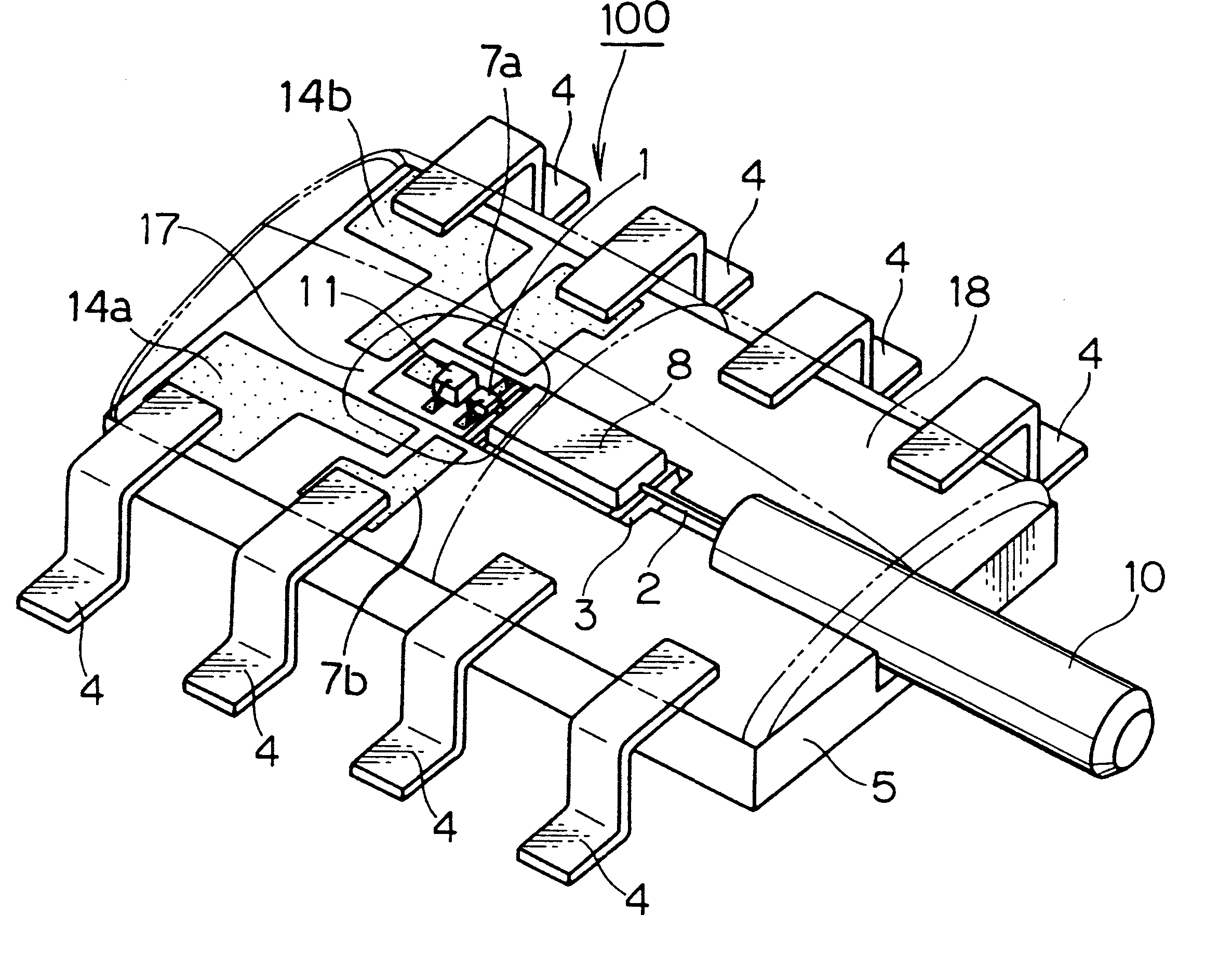
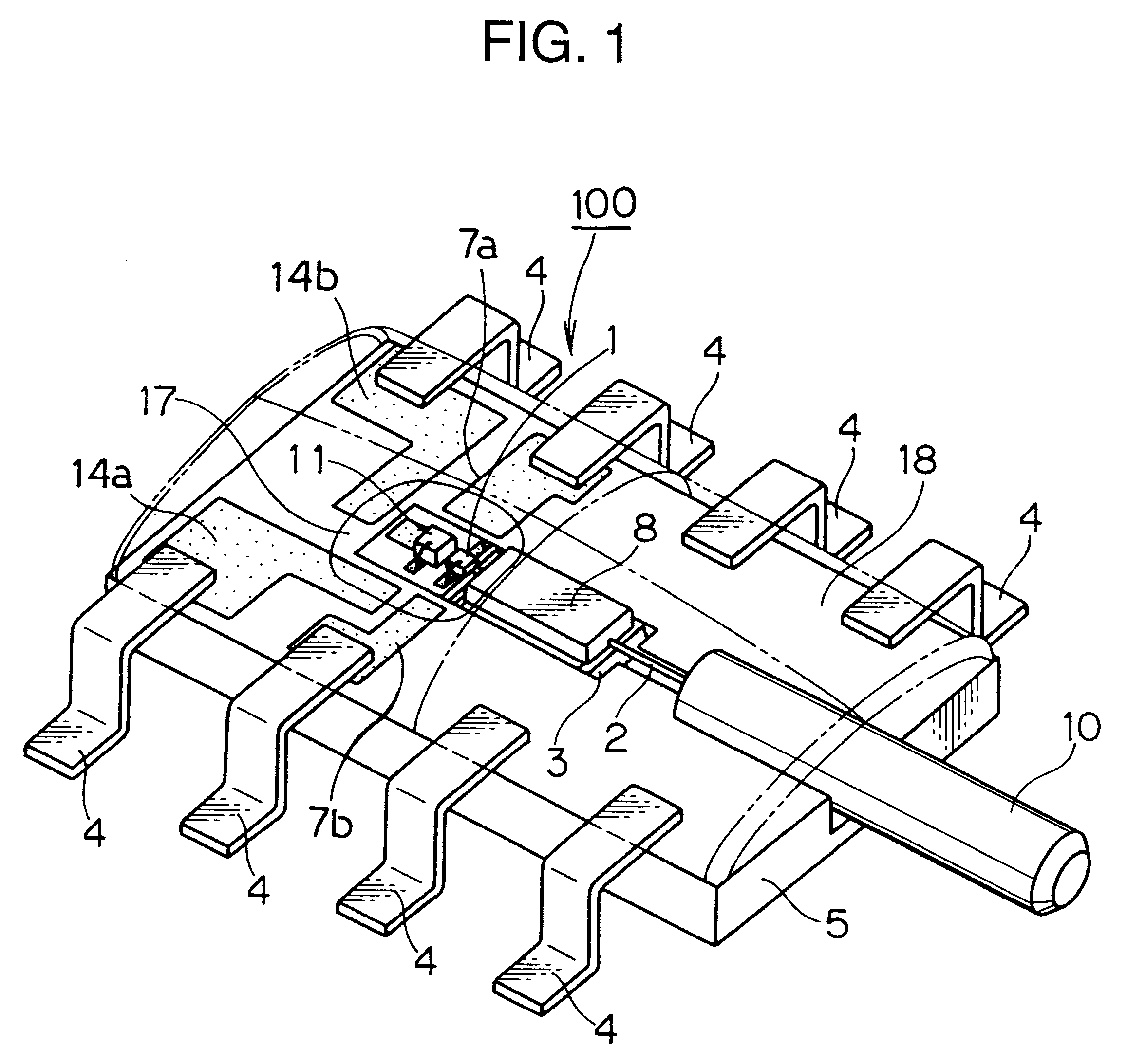
A first embodiment of the present invention is described. FIG. 1 shows a configuration of an optical interconnection module 100 in the first embodiment. FIG. 2 shows an exploded configuration of the optical interconnection module 100. FIG. 3 shows a sectional configuration of the optical interconnection module 100. FIG. 4 shows an appearance of the optical interconnection module 100.

As can be seen from the figures, the optical interconnection module 100 comprises a first mounting base member 3 and a second mounting base member 5. The first mounting base member 3 is made of, for example, a single crystalline silicon to which anisotropy etching can be processed. A light emitting device 1 such as a semiconductor laser, which is an example of an optical semiconductor device in the first embodiment, is fixed on the first mounting base member 3. The second mounting base member 5 is, for example, made of a ceramic material. Conductive patterns 7a, 7b, 14a and 14b are formed on a top surfac...

second embodiment

A second embodiment of the present invention is described. FIG. 5A shows a top appearance of an optical interconnection module 100A in the second embodiment, and FIG. 5B shows a bottom appearance of the optical interconnection module 100A. FIG. 6 shows a configuration of the optical interconnection module. FIG. 7 shows a sectional configuration of an optical interconnection portion of the optical interconnection module 100A.

A first mounting base member 103 is a single crystalline silicon substrate in which (100) surface of Miller indices corresponds to a principal plane. A V-shaped groove 109 on which an optical fiber 102 is held, a first cavity 106a in which a semiconductor laser 101 is contained, and a second cavity 106b in which a third mounting base member 119 is contained are respectively formed on the principal plane of the first mounting base member 103 by anisotropy etching. The third mounting base member 119 serves as a chip carrier.

The semiconductor laser 101, which is an ...

third embodiment

A third embodiment of an optical interconnection module in accordance with the present invention is described. FIG. 11 shows an appearance of a surface emitting laser which is a semiconductor device used in the third embodiment. FIG. 12 shows a configuration of a third mounting base member 219 used in the third embodiment. FIG. 13 show a configuration of an optical sub-assembly in the third embodiment. FIG. 14 shows a configuration of an optical interconnection module 200 in the third embodiment.

As shown in FIG. 11, the surface emitting laser 201 (hereupon, called "laser chip")is an array type VCSEL (Vertical Cavity Surface Emitting Laser) having four light emitting portions 220a, 220b, 220c and 220d. The laser chip 201 has a width of 250 .mu.m, a length of 1000 .mu.m, a thickness of 100 .mu.m, and a pitch of the light emitting portions of 250 .mu.m. Four electrodes 206a, 206b, 206c and 206d are respectively provided on a light emitting surface (front surface) of the laser 201 for s...


PUM


Abstract

In an optical interconnection module used for data communication, or the like, a semiconductor laser for emitting laser light and a photodiode for monitoring irradiation of the light by the laser are fixed on a first mounting base member made of a single crystalline silicon. An optical fiber is held on a V-shaped groove on the first mounting base member for facing the light emitting layer of the laser. At least a gap between the laser and the optical fiber is filled by a transparent resin having a refractive index equal to or larger than that of the optical fiber but smaller than the light wave guide layer of the laser. The transparent resin portion is further covered by non-transparent resin. The first mounting base member is fixed on a second mounting base member made of ceramic material having thermal expansion coefficient larger than that of the first mounting base but smaller than a circuit substrate made of epoxy resin.

Description

This application is based on patent applications 2000-054970, 2000-333609, and 2001-023415 filed in Japan, the contents of which are hereby incorporated by references.1. Field of the InventionThe present invention relates to an optical interconnection module used for optical data transmission and reception such as optical fiber communication.2. Description of the Related ArtIn a conventional optical interconnection module used for optical data communication, an optical semiconductor device such as a semiconductor laser for emitting light and an optical fiber optically interconnected to the laser are held on the same mounting substrate. Conductive patterns or electrodes are formed on the surface of the mounting substrate for supplying electric power to the optical semiconductor device. Furthermore, a V-shaped groove, on which the optical fiber is held, is formed on the mounting substrate. For realizing a desired interconnection efficiency, it is necessary to form the electrode and th...

Claims


Application Information

Patent Timeline
Patent Type & Authority Patents(United States)
IPC IPC(8): G02B6/42
CPCG02B6/421G02B6/4212G02B6/423G02B6/4232G02B6/4239G02B6/4292H01L2224/48091H01L2924/00014H01L2924/3025H01L2924/00G02B6/4267G02B6/4253G02B6/426G02B6/4274G02B6/4286G02B6/4243G02B6/4265
Inventor SETOGUCHI, KATSUHIDE
Owner KYOCERA CORP
Why Eureka
Try Eureka