Secure and dense SRAM cells in EDRAM technology

a sram cell, dense technology, applied in static storage, information storage, digital storage, etc., can solve the problems of soft errors, increased criticality of many aspects of operation, and inevitable scaling of individual elements

Inactive Publication Date: 2003-01-14
IBM CORP
View PDF9 Cites 26 Cited by
  • Summary
  • Abstract
  • Description
  • Claims
  • Application Information

AI Technical Summary

Benefits of technology

It is another object of the present invention to provide a technique of greatly reducing susceptibility to soft errors that can be implemented in arbitrary and / or existing memory cell designs.

Problems solved by technology

However, such scaling of individual elements inevitably increases criticality of many aspects of operation such as operation at reduced voltages, susceptibility to noise, heat dissipation and the like.
Among other problems aggravated by scaling, particularly in memory structures, is the problem of soft errors due to the transit of alpha particles through a memory cell.
Alpha particles are substantially unavoidable in the environment and their relatively high energy causes ionization which can introduce charge into the circuit in an unpredictable manner but without causing damage to the circuit element or impairing its function.
Scaling causes increased susceptibility to soft errors because it decreases the amount of charge required to induce a soft error through a number of mechanisms.
Further, numbers of soft errors per chip are increased by increased integration density.
That is, while soft errors are relatively rare and current memory cell designs are highly reliable and stable, such a memory can now be expected to experience a soft error, on average, every one to two months and may vary significantly (e.g. may double or more) with the logic state stored.
Unfortunately, most approaches to soft error correction compromise performance, especially processing speed, and / or integration density.
That is, error detection / correction circuits or redundant designs that have been used in the past to alleviate the problem of soft errors are either very expensive and / or very slow.
For example, some designs duplicate the cell array and, upon read out, picks the data with correct parity rather than performing a slow and complicated error detection and correction procedure even though such an approach more than doubles cost, limits usable memory capacity per chip and increases access time.
However, this approach does not provide protection against soft errors and, in fact, would provide only a marginal (10-50%) reduction in soft error rates while increasing production costs significantly.
The addition of further circuit elements such as resistor-capacitor circuits to increase stability of memory cells by reducing alpha particle induced transients have been proposed but would result in much larger cell size and much slower access time as well as increasing power consumption and heat dissipation requirements.
Neither of these proposals would avoid a need for error detection and correction circuitry which is slow and complicated; reducing overall processor performance.

Method used


Image

  • Secure and dense SRAM cells in EDRAM technology
  • Secure and dense SRAM cells in EDRAM technology
  • Secure and dense SRAM cells in EDRAM technology

Examples


Embodiment Construction

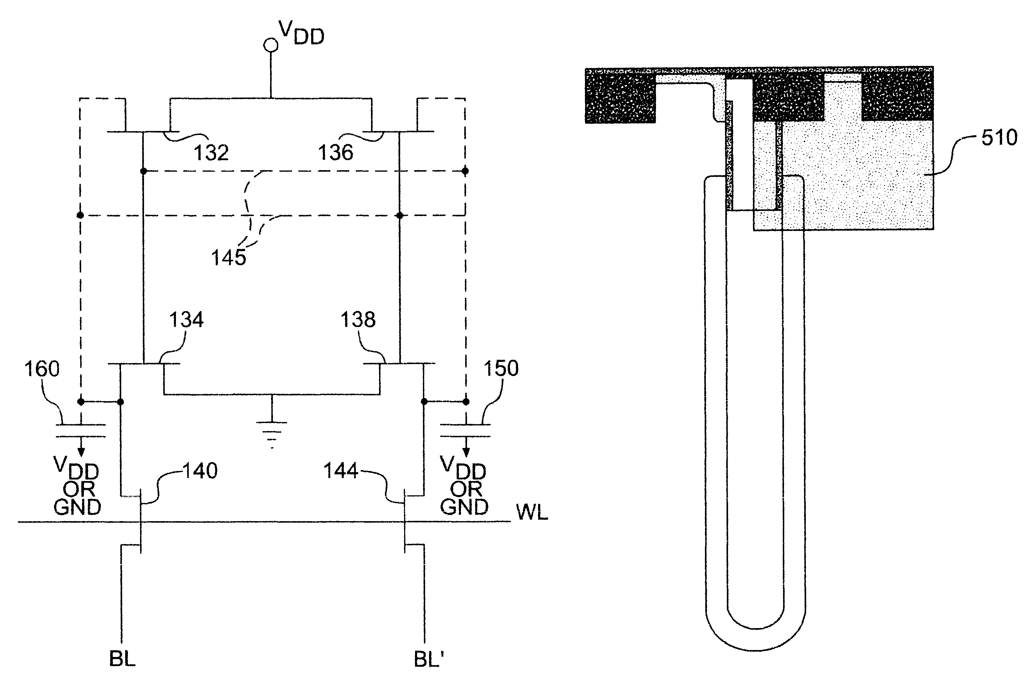
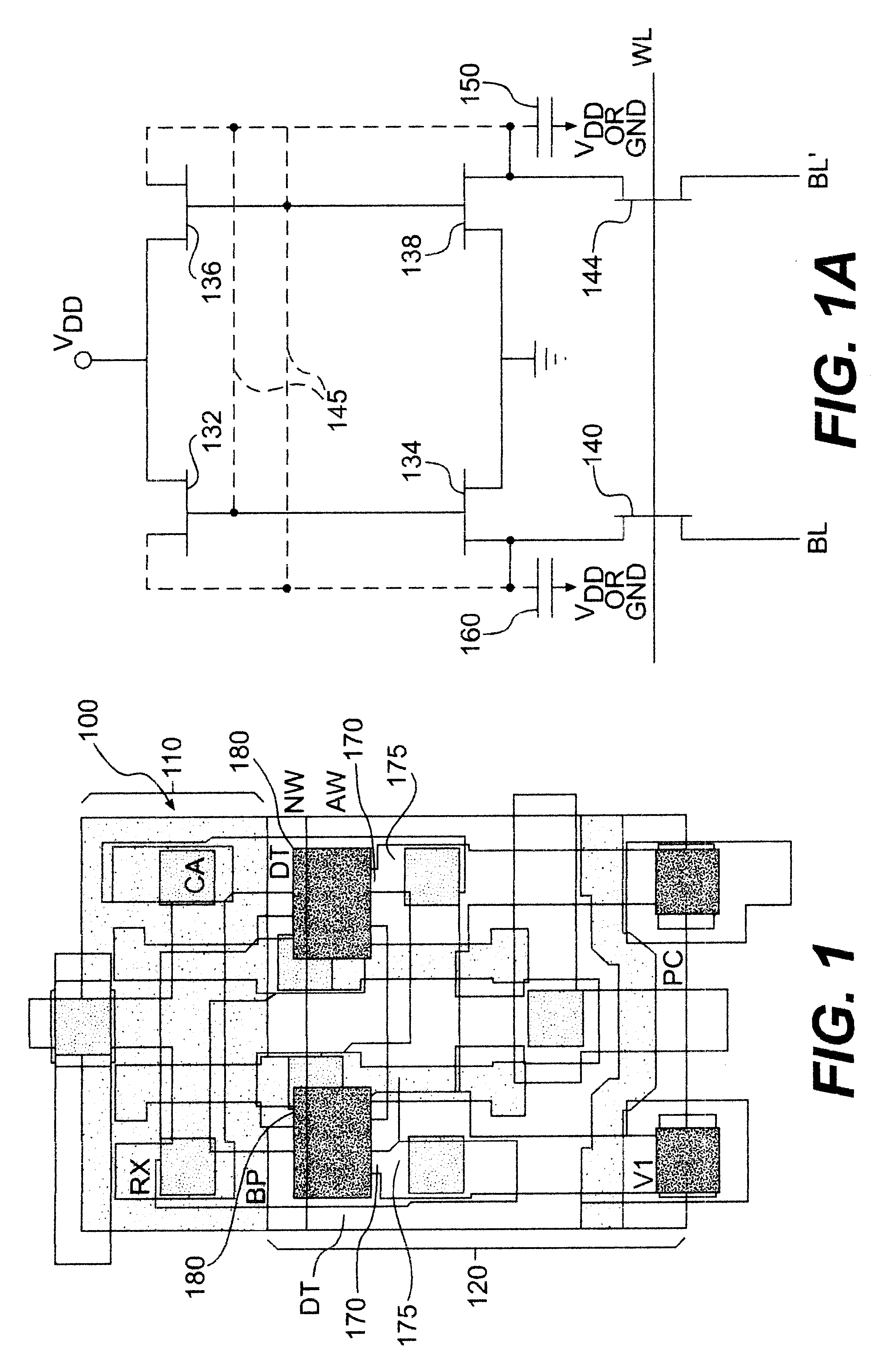
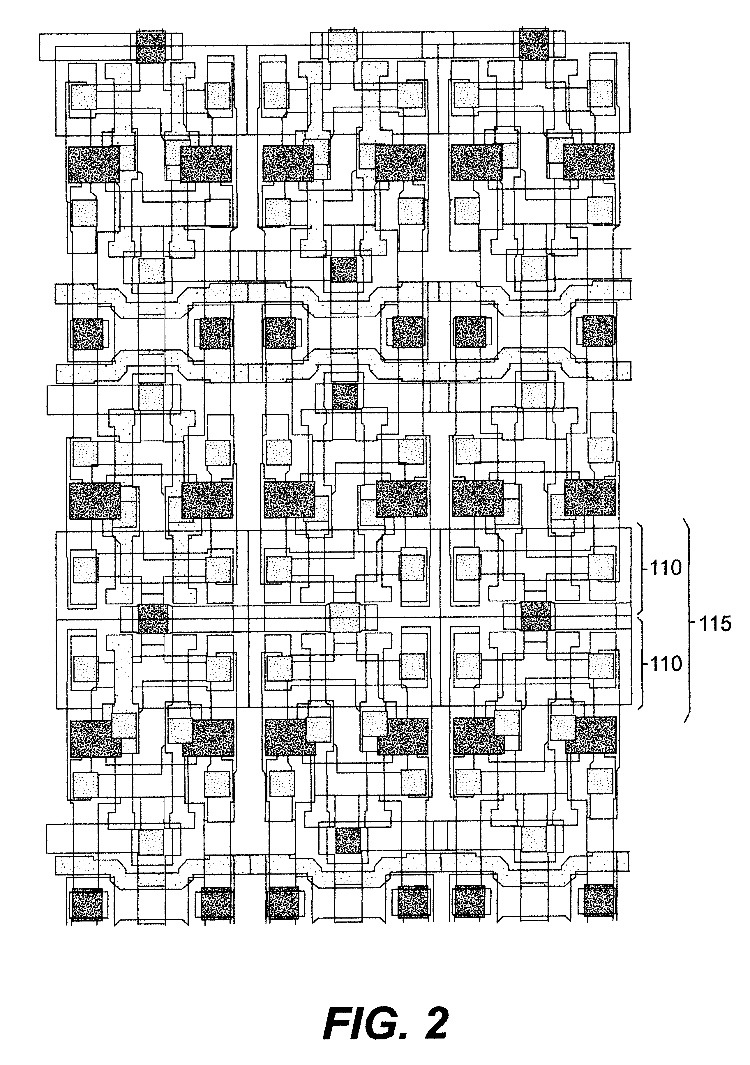
Referring now to the drawings, and more particularly to FIG. 1, there is shown, in plan view, the layout of an exemplary memory cell including the invention. It is to be understood that the invention can be implemented with arbitrary memory cell circuits or other active integrated circuits (e.g. registers, logic arrays, processors and the like) as will be demonstrated by discussion of FIGS. 1, 3 and 4, respectively, while FIG. 2 and the discussion thereof will demonstrate that the invention does not complicate or otherwise require any modification of the overall layout of the memory cell array on a chip.

Thus, those skilled in the art will be enabled to incorporate the invention, in accordance with its basic principles, to reduce soft error susceptibility in any memory cell and array design as well as other integrated circuits such as processors, logic arrays and the like. By the same token, it is to be understood that while similar memory cell layouts may be known and details thereo...


PUM


Abstract

Addition of capacitance to the storage nodes of static random access memory cells and other types of integrated circuits substantially increases Qcrit and substantially eliminates soft errors due to alpha particles; susceptibility to which would otherwise increase as integrated circuits are scaled to smaller sizes and manufactured at increased integration densities. Formation of the added capacitance as deep trench capacitors avoids any constraint on circuit or memory cell layout. Degradation of performance is avoided and performance potentially improved by permitting alteration of proportions of pull-down and pass gate transistors in view of the increased stability imparted by the added capacitors. One of the capacitor electrodes is preferably shorted to the supply voltage through an impurity well. Thus, the memory cell size can be reduced while greatly reducing susceptibility to soft errors; contrary to the effects of scaling at current and foreseeable feature size regimes.

Description

1. Field of the InventionThe present invention generally relates to high capacity static random access memories and other types of integrated circuits formed at high integration density and, more particularly, to achieving high levels of immunity to soft errors in such memories.2. Description of the Prior ArtSince the development of integrated circuits, the potential for reduced signal propagation time and increased functionality of individual chips as well as manufacturing economy has driven development of increases in integration density and scaling of individual circuit elements therein to smaller sizes. This incentive for scaling is particularly strong for memory devices which have approximately quadrupled in capacity every three years. However, such scaling of individual elements inevitably increases criticality of many aspects of operation such as operation at reduced voltages, susceptibility to noise, heat dissipation and the like.Among other problems aggravated by scaling, p...

Claims


Application Information

Patent Timeline
Patent Type & Authority Patents(United States)
IPC IPC(8): G11C11/412
CPCG11C11/4125
Inventor BARTH, JR., JOHN E.IYER, SUBRAMANIAN S.KHAN, BABAR A.WONG, ROBERT C.
Owner IBM CORP
Why Eureka
Try Eureka