Ball limiting metallurgy for input/outputs and methods of fabrication

a metallurgy and input/output technology, applied in the field of ball limiting metallurgy (blm) for input/output, can solve the problems of large shear stress on a wire lead or bump, intermetallic alloy brittleness, and easy stress cracking of intermetallic alloys

Inactive Publication Date: 2003-02-18
INTEL CORP
View PDF8 Cites 84 Cited by
  • Summary
  • Abstract
  • Description
  • Claims
  • Application Information

AI Technical Summary

Problems solved by technology

Power management and thermal management become very critical when wire leads or bumps are scaled down.
Elevated temperatures can also cause inter-diffusion of metals.
The resultant intermetallic alloys are brittle and may be susceptible to stress cracking.
A mismatch in the Coefficient of Thermal Expansion (CTE) can result in large shear stresses on a wire lead or bump.
Thermal cycling at lower thermal ramp rates may also cause a wire lead or bump to crack due to fatigue induced by elastic deformation or creep deformation.
Thus, the failure of I / Os, especially the power I / Os, due to high currents and high temperatures is a major concern.

Method used


Image

  • Ball limiting metallurgy for input/outputs and methods of fabrication
  • Ball limiting metallurgy for input/outputs and methods of fabrication
  • Ball limiting metallurgy for input/outputs and methods of fabrication

Examples


first embodiment

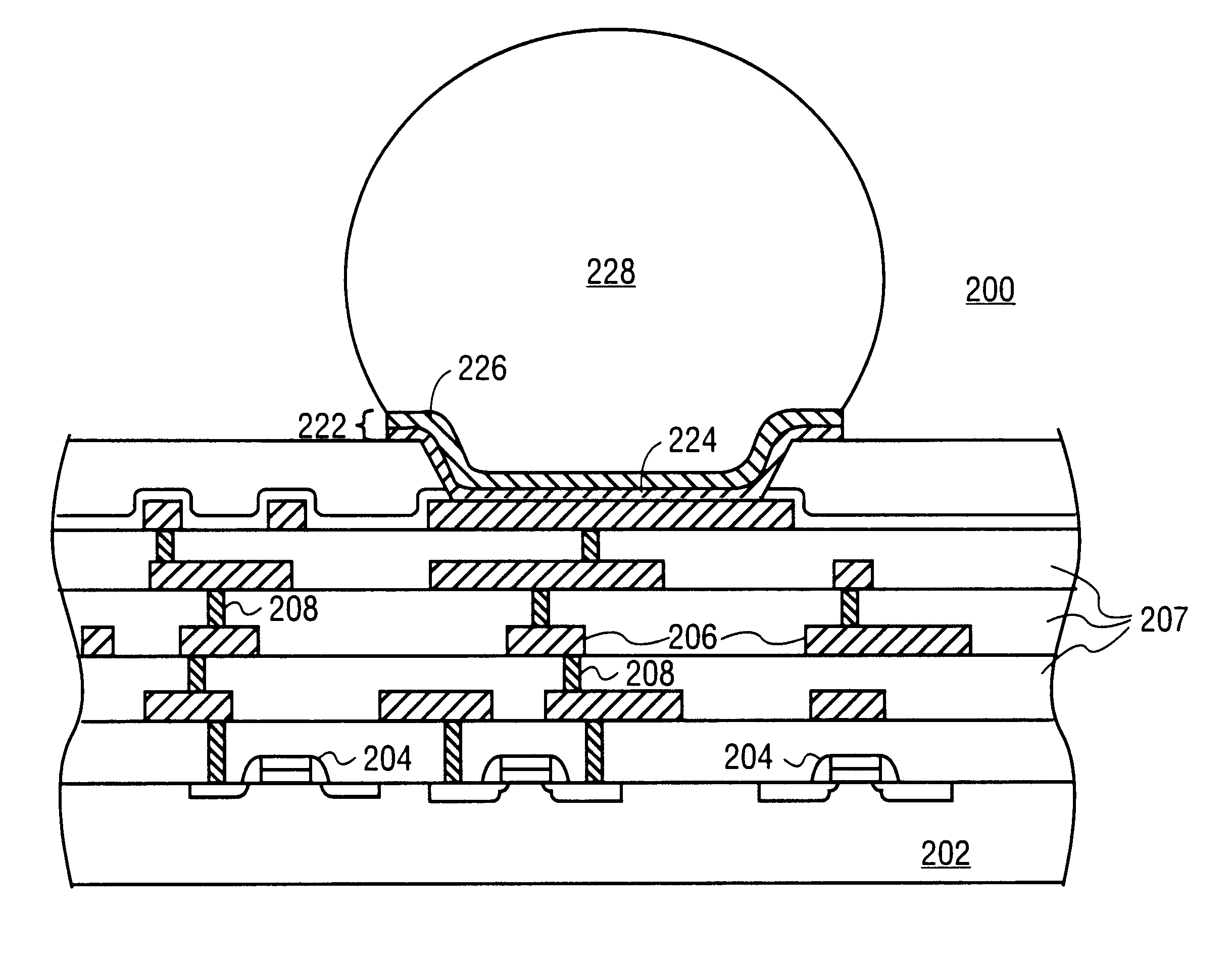
According to the present invention the ball limiting metallurgy (BLM) includes an upper layer 226 which is wettable by solder. According to the present invention the upper lay 226 is a film consisting of nickel, vanadium, and nitrogen. Nitrogen is added to the film to lock the vanadium with nitrogen so that it cannot react with oxygen and degrade the reliability of the BLM. The upper layer 226 includes a suitable amount of nitrogen to sufficiently prevent the oxidation of vanadium in the upper film 226. In an embodiment of the present invention the upper film includes as much nitrogen as vanadium. In an embodiment of the present invention the upper film 226 includes about 8 atomic percent vanadium, about 8 atomic percent nitrogen, and the remainder nickel. The upper nickel-vanadium-nitrogen alloy film 226 can have a thickness between 1000-4000 .ANG..

A suitable nickel-vanadium-nitrogen alloy film 226 can be formed by reactive sputtered utilizing a nickel-vanadium target in an ambient...

second embodiment

In the present invention the upper layer of 226 of BLM 222 is a nickel-niobium (Ni--Nb) alloy. In an embodiment of the present invention the upper layer 226 is a nickel-niobium (Ni--Nb) alloy having approximately 10 atomic percent niobium (Nb) with the remainder nickel (Ni). A nickel-niobium (Ni--Nb) alloy having a thickness between 1000-4000 .ANG. can be used. A suitable nickel-niobium (Ni--Nb) film can be formed by any well-known method such as by sputtering from a nickel-niobium (Ni--Nb) target. A nichel-niobium (Ni--Nb) upper film 226 has shown good reliability.

The BLM 222 acts a diffusion barrier to metals. Depending upon the type of metallurgy selected for bumps and the BLM, additional layers may be inserted between the adhesion 224 and the upper layer 226. The intermediate layer used must have good adhesion to both the adhesion layer 224 and the upper layer 226.

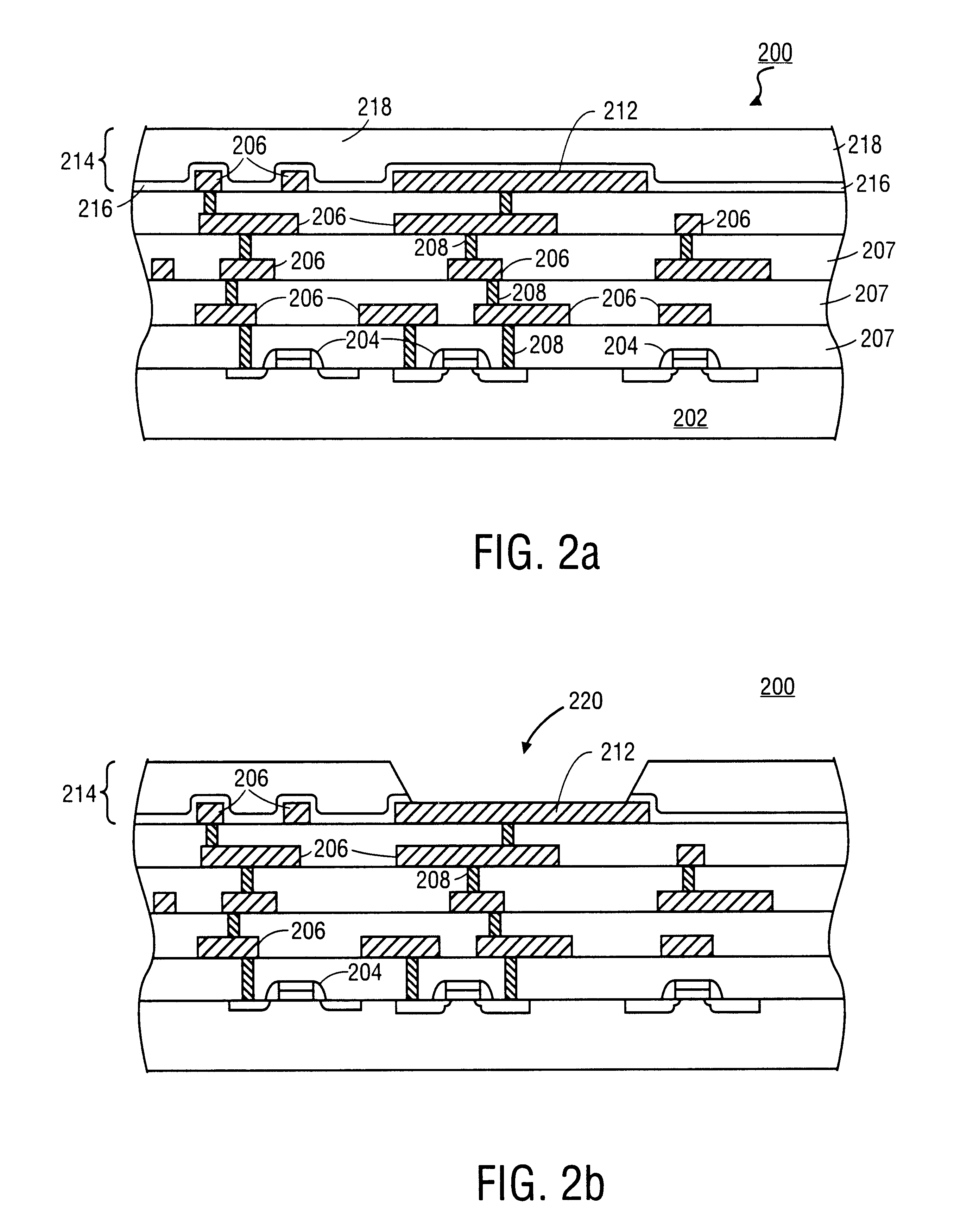
Next, a bump 228 is formed on BLM layer 222 over bond pad 212. A bump 228 can be formed, by for example, forming a p...


PUM

PropertyMeasurementUnit
thickaaaaaaaaaa
thicknessaaaaaaaaaa
diameteraaaaaaaaaa

Abstract

The present invention is an input / output for a device and it method of fabrication. The input / output of the present invention comprises a bond pad having a ball limiting metallurgy (BLM) formed thereon and a bump formed on the ball limiting metallurgy (BLM). In an embodiment of the present invention the ball limiting metallurgy comprises a first film comprising nickel, vanadium, and nitrogen. In the second embodiment of the present invention the bump limiting metallurgy includes a first alloy film comprising a nickel-niobium alloy.

Description

1. Field of the InventionThe present invention relates to the field of semiconductor Integrated Circuits (IC), and more specifically, to a bump limiting metallurgy (BLM) for input / output of a device.2. Discussion of Related ArtInput / outputs are used in a device to condition and distribute power, ground, and signals. The I / Os can be wirebonded to a package or board with leads formed from Gold (Au) or Copper (Cu) wire. However, when the number of I / Os reaches about 400 to 1000, bumping often becomes more advantageous than wirebonding.FIG. 1(a) and FIG. 1(b) show a solder bump 15 with a diameter 1 and a pitch 2. The solder bump 15 is formed on Ball Limiting Metallurgy (BLM) 14. BLM is also known as Pad Limiting Metallurgy (PLM) or Under Bump Metallurgy (UBM). The BLM 14 is connected through a via 12 in the passivation layer 13 to an underlying bond pad 11b. The passivation layer 13, comprises one or more layers of materials, such as silicon oxide, silicon nitride, or polyimide, which a...

Claims


Application Information

Patent Timeline
Patent Type & Authority Patents(United States)
IPC IPC(8): H01L21/02H01L21/60H01L23/485H01L23/48
CPCH01L24/11H01L24/13Y10T428/12556H01L2224/13099H01L2924/01002H01L2924/01013H01L2924/01015H01L2924/01018H01L2924/0102H01L2924/01022H01L2924/01029H01L2924/01033H01L2924/01049H01L2924/01057H01L2924/01073H01L2924/01074H01L2924/01078H01L2924/01079H01L2924/01082H01L2924/01322H01L2924/01327H01L2924/14H01L2924/1433H01L2924/19041H01L2924/19043H01L2924/30107H01L2924/01005H01L2924/01006H01L2924/01023H01L2924/01024H01L2924/01041H01L2924/01076H01L2924/014H01L2924/00013H01L2224/1147H01L2924/0001H01L2224/13111H01L2224/13109H01L2224/131H01L2224/29099H01L2924/00014H01L2924/15787H01L2224/05027H01L2224/05022H01L2224/05001H01L2224/05572H01L2224/05172H01L24/03H01L24/05H01L2924/00H01L2224/05655H01L2224/05166H01L2224/05171H01L2224/05184
Inventor SESHAN, KRISHNA
Owner INTEL CORP
Why Eureka
Try Eureka