

Process for the surface polishing of silicon wafers
a technology of surface polishing and silicon wafers, applied in other chemical processes, lapping machines, manufacturing tools, etc., can solve the problems of silicon wafers, certain number of surface defects which cannot be cleaned off, and significantly lower material removal rates than stock-removal polishing processes
- Summary
- Abstract
- Description
- Claims
- Application Information
AI Technical Summary
Benefits of technology
Problems solved by technology
Method used
Image

Examples
invention
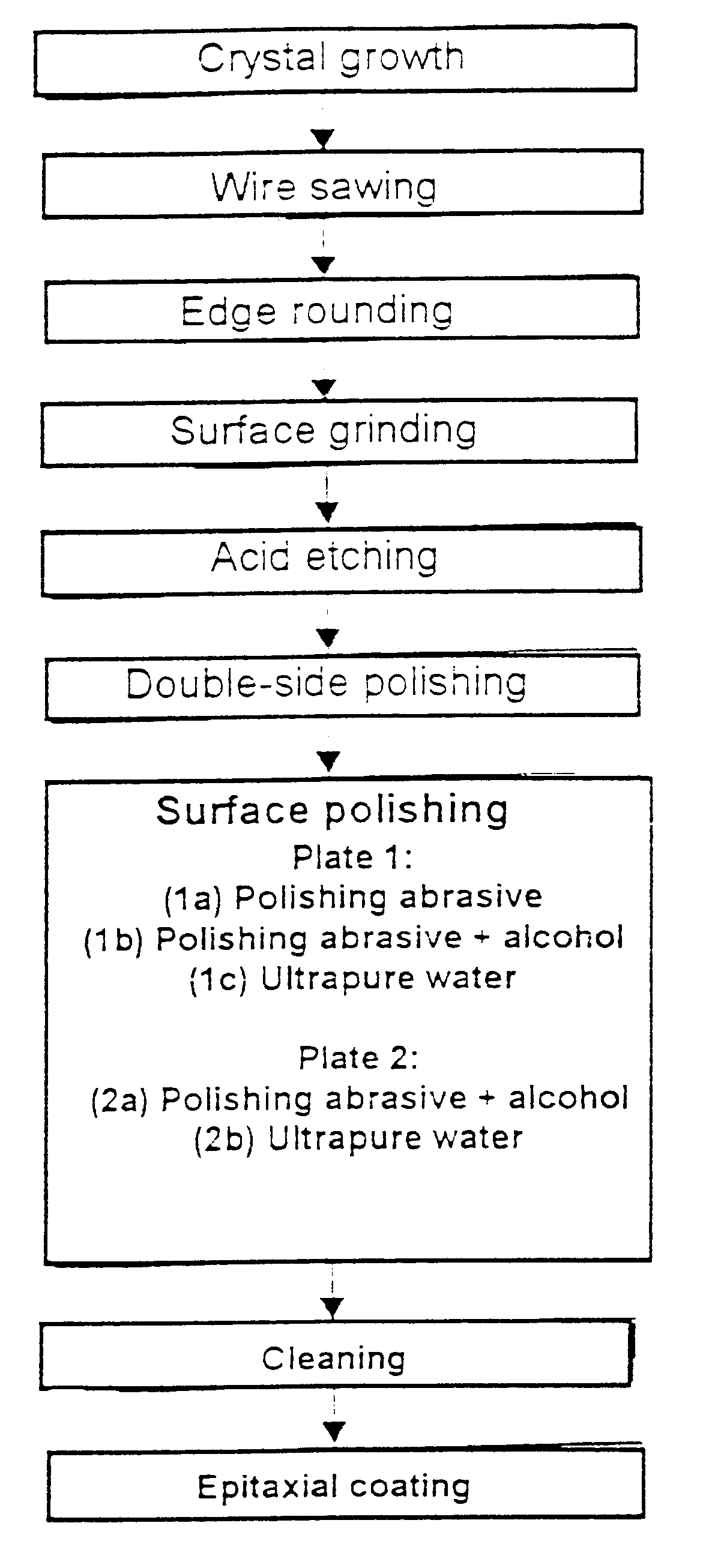
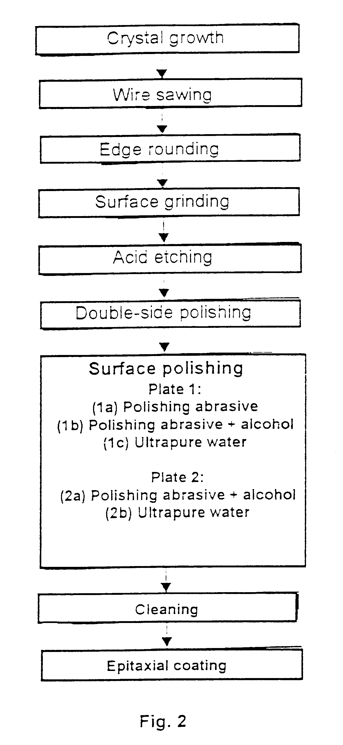
EXAMPLE (INVENTION)
The procedure utilized was analogous to that used in the Comparative Example. The following procedure was selected for the surface polishing, with the same polishing cloths being used. First of all, on plate 1, polishing was once again carried out with LEVASIL 300.RTM. (3% by weight of SiO.sub.2 ; pH 10.5), this time for 120 sec. Then, a polishing abrasive which comprised an aqueous suspension of pyrogenic silica (SiO.sub.2 particle size 30-40 nm; solid content 1.5% by weight; NH.sub.4 OH-stabilized), to which 0.2% by volume of triethylene glycol had been admixed and which had a pH of 9.7, was added for 40 sec. Then, ultrapure water was supplied for 20 sec. On plate 2, with an otherwise identical procedure to that utilized in the Comparative Example, the same suspension of pyrogenic silica with added triethylene glycol as on plate 1 was used. The total amount of silicon removed from the front surface of the silicon wafer was this time on average 0.5 .mu.m, of whic...
PUM
| Property | Measurement | Unit |
|---|---|---|
| grain diameter | aaaaa | aaaaa |
| grain diameter | aaaaa | aaaaa |
| size | aaaaa | aaaaa |
Abstract
Description
Claims
Application Information