Semiconductor light-emitting element
a technology of light-emitting elements and semiconductors, applied in the direction of basic electric elements, semiconductor devices, electrical equipment, etc., can solve the problems of high cost, difficult to employ white leds for illumination use, and inability to recognize full color by whi
- Summary
- Abstract
- Description
- Claims
- Application Information
AI Technical Summary
Benefits of technology
Problems solved by technology
Method used
Image
Examples
example 1
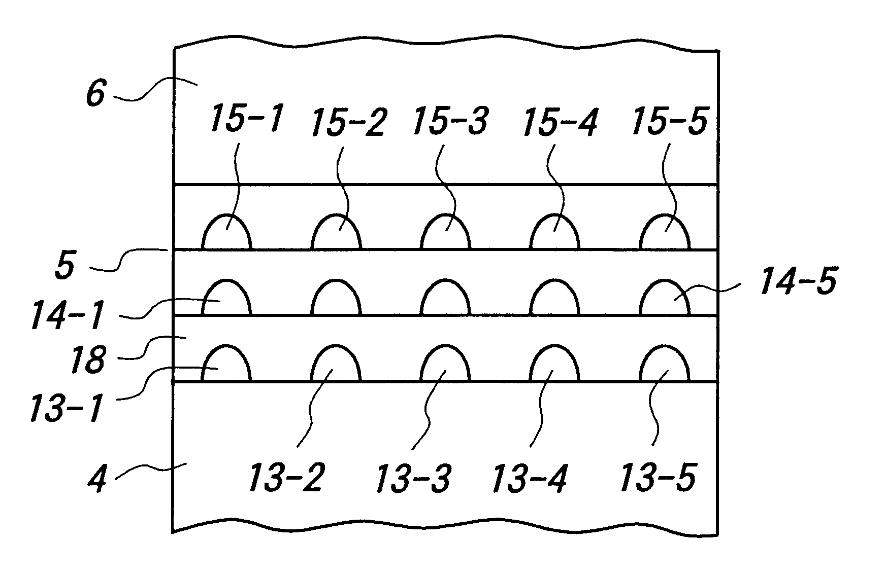
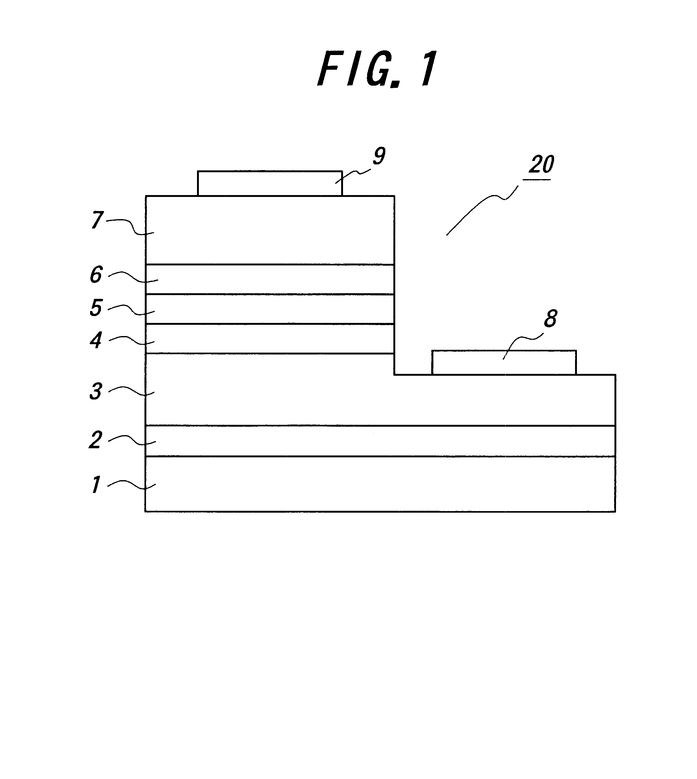
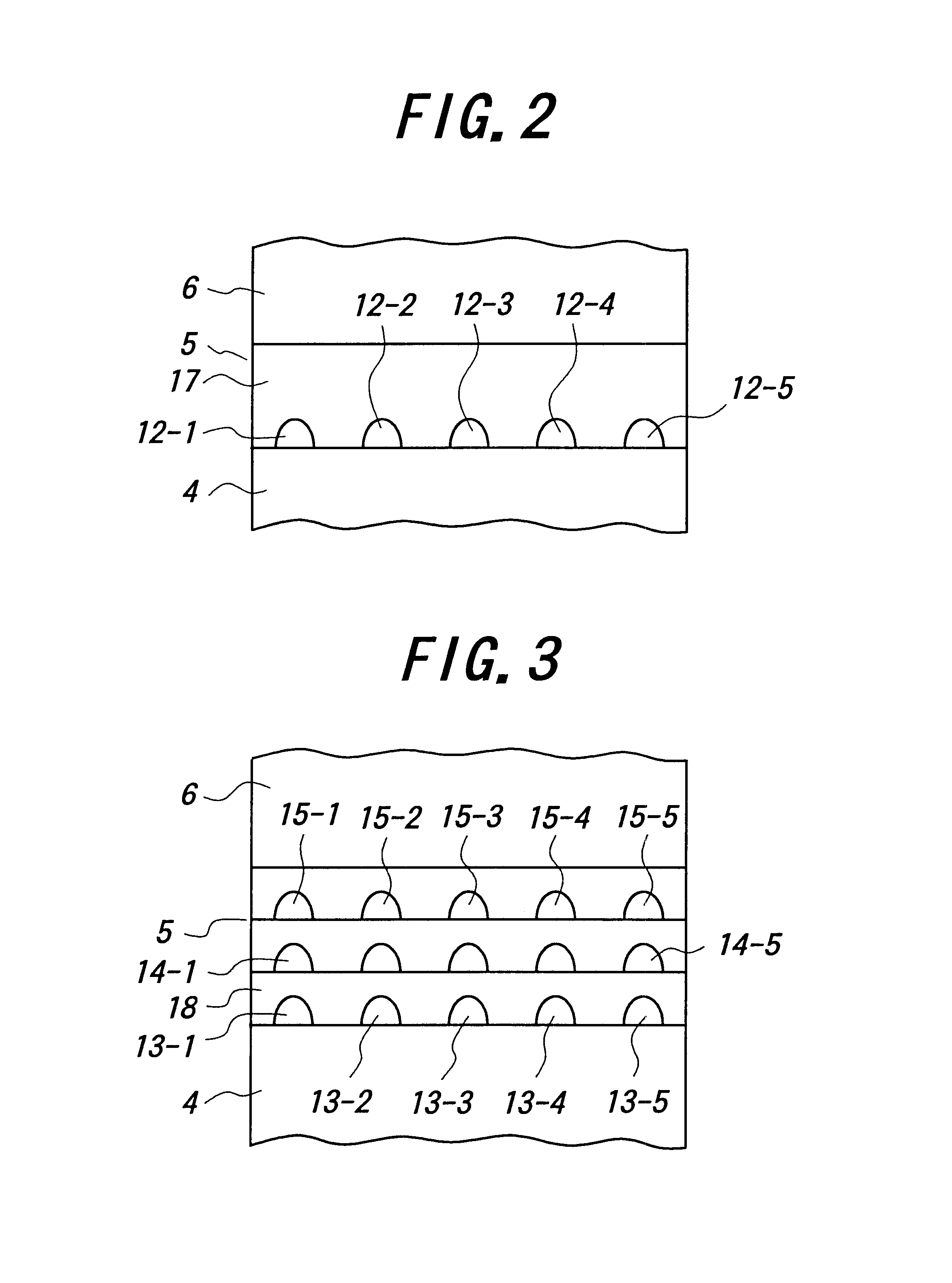
A sapphire single crystal substrate having a diameter of 2 inches and a thickness of 430 .mu.m was employed, and thus, pre-treated by H.sub.2 SO.sub.4 +H.sub.2 O.sub.2, and set into a MOCVD apparatus. To the MOCVD apparatus was attached a gas system of NH.sub.3, TMA, TMG and SiH.sub.4. Then, the substrate was heated to 1200.degree. C., and an ammonia gas (NH.sub.3) was flown with a H.sub.2 carrier gas for five minutes, to nitride the main surface of the substrate. In ESCA analysis, it was turned out that a surface-nitriding layer was formed on the main surface by the surface-nitriding treatment, and the nitrogen content at the depth of 1 nm from the main surface was seven atomic percentages.
Then, TMA and NH.sub.3 were flown at an average rate of 10 m / sec, with flowing H.sub.2 gas at 10 m / sec, to form an AlN film in a thickness of 1 .mu.m as an underlayer. The full width at half maximum in X-ray rocking curve of the AlN film was 90 seconds, and thus, the good crystallinity of the AlN...
example 2
Except that the island-shaped single crystal portions were formed of Er, Tm, Pr and Eu doped In.sub.0.1 Ga.sub.0.9 N in a thickness of 20 .ANG. and a diameter of 100 .ANG., and thereafter, Eu, Er, Tm elements were irradiated and adsorbed at the boundary between the island-shaped single crystal portions and the first cladding layer as an underlayer through the molecular beam irradiation from their respective solid raw material sources, a semiconductor light-emitting element was fabricated in the same manner as Example 1.
Then, when a voltage of 3.5V was applied between the p-type electrode and the n-type electrode and thus, a current of 20 mA was flown through the semiconductor light-emitting element, a white light was generated and emitted from the semiconductor light-emitting element at a luminescence efficiency of 100 lm / W.
As is apparent from Examples 1 and 2, it is confirmed that the semiconductor light-emitting element of the present invention is usable as a practical white LED. ...
PUM
| Property | Measurement | Unit |
|---|---|---|
| thickness | aaaaa | aaaaa |
| thickness | aaaaa | aaaaa |
| thickness | aaaaa | aaaaa |
Abstract
Description
Claims
Application Information
 - R&D
- Intellectual Property
- Life Sciences
- Materials
- Tech Scout
- Unparalleled Data Quality
- Higher Quality Content
- 60% Fewer Hallucinations
Browse by: Latest US Patents, China's latest patents, Technical Efficacy Thesaurus, Application Domain, Technology Topic, Popular Technical Reports.
© 2025 PatSnap. All rights reserved.Legal|Privacy policy|Modern Slavery Act Transparency Statement|Sitemap|About US| Contact US: help@patsnap.com


