Method and apparatus for a network-based mask defect printability analysis system

a network-based mask and printability technology, applied in the field of integrated circuit manufacturing, can solve the problems of not being able to perfectly reproduce the design serif 215 shape on the mask material, mask defects occur outside the controlled process, and are unrealistic to assume, so as to achieve the effect of solving problems and decision-making

Inactive Publication Date: 2003-06-10
SYNOPSYS INC
View PDF54 Cites 166 Cited by
  • Summary
  • Abstract
  • Description
  • Claims
  • Application Information

AI Technical Summary

Benefits of technology

To communicate with the client view stations, the simulation server includes a network server. In one embodiment, the network server is programmed with open source software. By using open source software, the code for implementing the network server is extremely robust with minimal additional cost to the total system.
In the present invention, users at the client view stations can simultaneously view the analysis being done on the mask image. In one embodiment, users can communicate during this analysis, thereby providing the users a valuable opportunity for problem solving and decision-making.

Problems solved by technology

It is, unfortunately, unrealistic to assume that the electron beam and other machines used to manufacture these masks can do so without error.
In the typical manufacturing process, some mask defects do occur outside the controlled process.
This is because the size of the serifs is very small----they are designed to be smaller than the optical resolution of the lithography process to be used----and the electron beam typically can not perfectly reproduce the design serif 215 shape onto the mask material.
However, not all mask defects are important with respect to the desired end result----the end result being an-accurate representation of the original design layout on the photoresist material or etched into silicon.
Due to these changes, conventional methods of, inspection are rapidly proving to be inadequate because they do not address several issues.
First, whether a defect prints or not greatly depends on both its location and size, not just size or transmission / reflection characteristics alone.
Second, advanced OPC mask features can trigger false defect detections.
Although some existing mask inspection tools have a sliding scale setting to "tolerate" OPC features this is not a robust method since defects associated with these special features may be overlooked because of this arbitrary scale.
Additionally, OPC features are typically designed for a specific set of stepper parameters, but conventional tools, sliding scales are blind to these optical parameters.
Third, phase information is not properly incorporated into consideration, if at all, in the typical conventional defect inspection scheme.
Therefore, phase shifting masks are not properly inspected.
Finally, even though a defect may not appear to print, it might affect the process latitude in a way that will decrease yield and not be detected by conventional on-line defect inspection, systems.
On the other hand,. off-line inspection stations, which either scan for defects directly or review previously stored undeterminable defect data from an on-line tool, also face the same issues.
In addition, these issues may require expensive engineers' time to be resolved, and thus diminish throughput while raising cost.
Although with an engineer's judgement, magnitude of the defect printability / classification problem is greatly reduced due to experience and know-how, still, there is not enough certainty and accuracy until the defect is viewed as it appears on an actual wafer after exposure through the mask.
Thus, using currently existing inspection systems, it is nearly impossible to judge a defect's printability without actually printing the mask onto a wafer, which is expensive and time-consuming.

Method used


Image

  • Method and apparatus for a network-based mask defect printability analysis system
  • Method and apparatus for a network-based mask defect printability analysis system
  • Method and apparatus for a network-based mask defect printability analysis system

Examples


Embodiment Construction

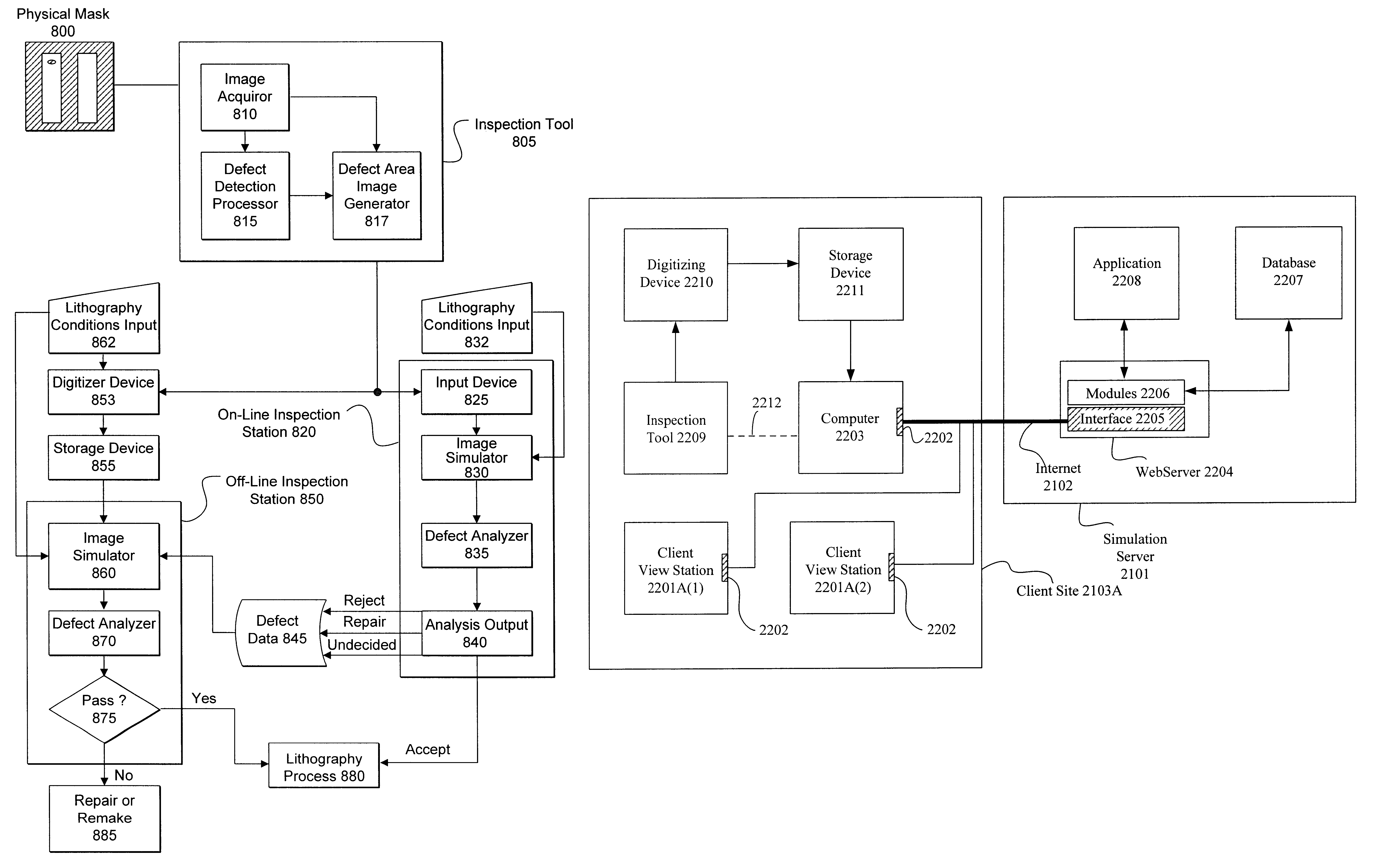
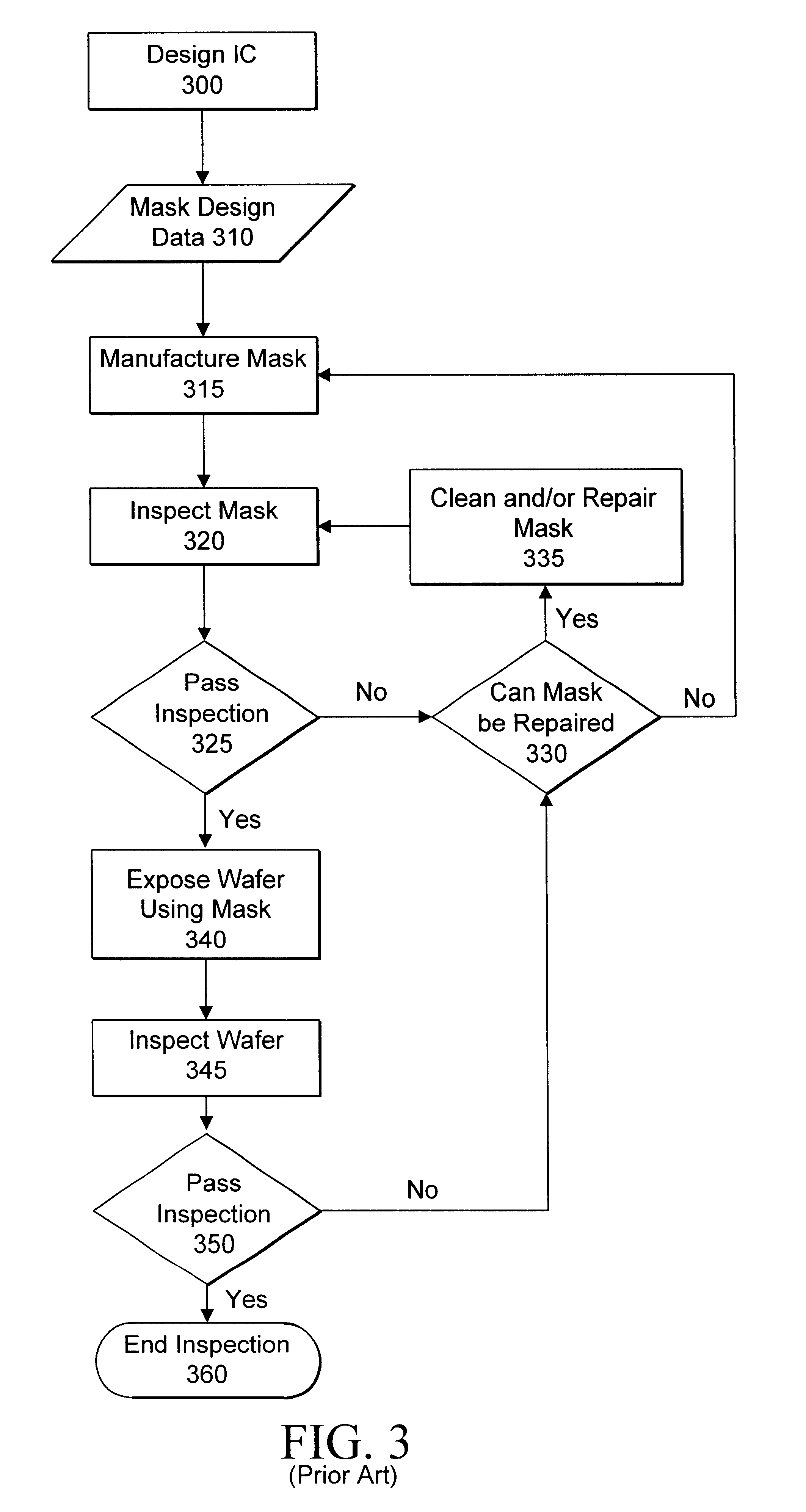
Photolithography is a process whose input is a mask and whose output is the printed patterns on a wafer. The printed result from a mask is what design engineers, lithographers, and mask manufacturers really care about. Using prior methods, the only way to inspect this printed result was to perform an actual wafer exposure and therefore incur potentially unnecessary costs in time and money. The present invention solves some of the problems of these prior methods by providing for mask inspection that takes printability into account without the need for the expensive steps of actually exposing a wafer. The present invention is capable of using a captured image of a mask----that accurately enough represents the physical mask (i.e. such as from a high resolution optical microscope or a scanning electron microscope)----and using that captured image to simulate the wafer exposure that the mask would provide under a given set of stepper conditions. Thus, when an initial mask inspection for ...


PUM

PropertyMeasurementUnit
mask defect analysisaaaaaaaaaa
area networkaaaaaaaaaa
areaaaaaaaaaaa

Abstract

A mask defect printability simulation server provides simulations, one-dimensional analysis, and reports to multiple clients over a wide area network, such as the Internet. This network-based simulation server allows a client to leverage a core of highly-trained engineers. Additionally, the network-based simulation server can be easily supported since only a single source for the tools associated with the simulation server is necessary for multiple clients. A client can access the simulation server using a standard personal computer having a browser, thereby eliminating the need for client to maintain an expensive database for the server. Finally, in the network-based simulation server, multiple users can view the same mask defect image and provide real-time comments to each other as simulation and analysis are performed on the defect image, thereby encouraging problem solving and decision-making dialogue among the users.

Description

THE BACKGROUND OF THE INVENTIONa. The Field of the InventionThis invention relates to the field of integrated circuit manufacturing. In particular, the invention relates to a system for inspection of defects on masks used in the manufacture of integrated circuits.b. Description of Related ArtIn designing an integrated circuit (IC), engineers typically rely upon computer simulation tools to help create a circuit schematic design consisting of individual devices coupled together to perform a certain function. To actually fabricate this circuit in a semiconductor substrate the circuit must be translated into a physical representation, or layout, which itself can then be transferred onto a template (i.e., mask), and then to the silicon surface. Again, computer aided design (CAD) tools assist layout designers in the task of translating the discrete circuit elements into shapes which will embody the devices themselves in the completed IC. These shapes make up the individual components of ...

Claims


Application Information

Patent Timeline
Patent Type & Authority Patents(United States)
IPC IPC(8): G03F7/20G03F1/00G06F17/50G03F7/14G01Q30/02G01Q30/04G01Q60/18G01Q60/24G01Q80/00G01Q90/00G03F1/26G03F1/36G03F1/84G06T7/00H01L21/027
CPCG03F1/26G03F1/84G03F7/70441G03F7/705G06T7/0004G06F17/5068G03F1/36Y10S977/839G06T2207/30148Y10S977/887Y10S977/953G06F30/39
Inventor PANG, LINYONGHOWARD, DANIEL WILLIAMKARKLIN, LINARD
Owner SYNOPSYS INC
Why Eureka
Try Eureka