Organic electronic devices having conducting self-doped polymer buffer layers

a technology of organic electronic devices and buffer layers, which is applied in the direction of discharge tubes/lamp details, discharge tubes luminescnet screens, other domestic articles, etc., can solve the problems of exacerbate performance failures that can occur, shadowed regions close to particles, and dark spots which can grow into larger and larger nons, so as to increase performance reliability

Inactive Publication Date: 2003-08-26
3M INNOVATIVE PROPERTIES CO
View PDF37 Cites 43 Cited by
  • Summary
  • Abstract
  • Description
  • Claims
  • Application Information

AI Technical Summary

Benefits of technology

The present invention relates to adding a buffer layer, comprising a self-doped polymer, adjacent to an electrode layer in an organic electronic device. The invention further relates to adding a buffer layer, comprising an intrinsically conducting polymer having no mobile counterions, adjacent to an electrode layer in a small molecule, molecularly doped polymer, or conjugated polymer organic light emitting diode. For example, a buffer layer may be added between the anode layer and hole transporting layer of an organic electronic device to increase performance reliability. A buffer layer could also be added between a substrate and cathode layer.
When the buffer layer of the present invention is used in an organic electronic device such as an organic light emitting diode (OLED), the benefits to performance reliability include reducing or eliminating performance failures such as electrical shorts and non-radiative regions (dark spots). Typical performance failures are described in Antoniadas, H., et al., "Failure Modes in Vapor-Deposited Organic LEDs," Macromol. Symp., 125, 59-67 (1997). The performance reliability of OLEDs can be influenced by a number of factors. For example, defects in, particles on, and general variations in the morphology at the surface of the materials comprising the substrate and electrode layers can cause or exacerbate performance failures that can occur in OLEDs. Particles or defects on the surface of the substrate or electrode layer may prevent the electrode surface from being coated uniformly during the deposition process. This can cause shadowed regions close to the particle or defect. Shadowed areas provide pathways for water, oxygen, and other detrimental agents to come into contact with and degrade the various lamp layers. This degradation can lead to dark spots which can grow into larger and larger non-emissive regions. This degradation can lead to immediate device failure due to electrical shorting or slower, indirect failure caused by interaction of the OLED layers with the atmosphere. The planarization provided by a conformal buffer layer can mitigate these imperfections.
An advantage of at least one embodiment of the present invention is the reduction or elimination of mobile counterions in an organic electronic device. Preferably, counterion mobility is reduced or eliminated in the buffer layer of such a device. It is advantageous to immobilize these counterions because it is believed that they can migrate in the electrode structure and interfere with the movement of positive charges or electrons in the device.
Another advantage of at least one embodiment of the present invention is the avoidance of undesirable operating voltage increase over time.
Another advantage of at least one embodiment of the present invention is increased device lifetime and higher operating reliability.
As shown in FIG. 3, when an externally doped polymer (polyaniline containing sulfonic acid dopant, obtained as an experimental sample from Monsanto Chemical Co., St. Louis, Mo.) was used as a buffer layer on an anode-coated substrate in an operating OLED, the voltage increased from about 5.6 to 7.4 volts over about 20 hours at a constant current density of 20 milliAmps / square centimeter (mA / cm.sup.2). FIG. 3 also shows that a similar device having no buffer layer did not exhibit the same voltage increase. The OLED having no buffer layer showed no voltage increase during the initial 20 hours of operation, and an increase from about 5.5 to about 5.7 volts during 45 hours of operation at a constant current density of 20 mA / cm.sup.2. This data suggests that the voltage increase is caused by the externally-doped polymer buffer layer. FIG. 4 shows that a device of the invention having a buffer layer comprising a conducting self-doped polymer (water-soluble sulfonated self-doped polyaniline obtained from Aldrich) instead of an externally doped polymer did not have a substantial voltage increase over time, and, in fact, had a voltage profile comparable to that of a device having no buffer layer. The OLED comprising a self-doped polymer buffer layer showed a voltage increase from about 6.3 to 6.5 volts during the initial 20 hours of operation, from about 6.3 to 6.6 volts during 45 hours of operation, and an increase from about 6.3 to 7.2 volts during 100 hours of operation, at a constant current density of 20 mA / cm.sup.2. Accordingly, the present invention provides the advantages of a buffer layer without the disadvantages of an externally-doped polymer buffer layer.

Problems solved by technology

For example, defects in, particles on, and general variations in the morphology at the surface of the materials comprising the substrate and electrode layers can cause or exacerbate performance failures that can occur in OLEDs.
This can cause shadowed regions close to the particle or defect.
This degradation can lead to dark spots which can grow into larger and larger non-emissive regions.
This degradation can lead to immediate device failure due to electrical shorting or slower, indirect failure caused by interaction of the OLED layers with the atmosphere.
Adding a buffer layer comprising an externally-doped polymer to an organic electronic device can cause an undesirable increase in operating voltage over time.

Method used


Image

  • Organic electronic devices having conducting self-doped polymer buffer layers
  • Organic electronic devices having conducting self-doped polymer buffer layers
  • Organic electronic devices having conducting self-doped polymer buffer layers

Examples


example 1

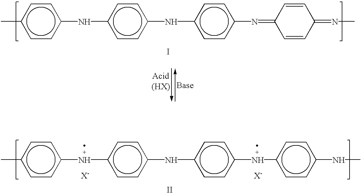
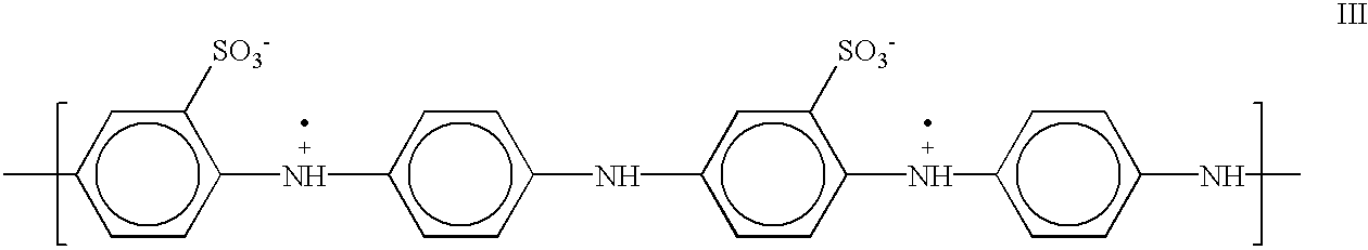
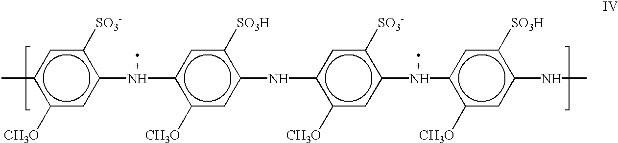
OLED With Self-doped Polyaniline

An OLED device was constructed according to the method of Comparative Example 1, except the substrate was treated with an oxygen plasma for 4 minutes at 50 Watts and 200 millitorr of oxygen in a reactive ion etcher (Micro-RIE series 80, Technics, Inc., Dublin, Calif.) and a 600 .ANG. layer of self-doped water soluble polyaniline (Aldrich) was used in place of the externally doped polyaniline. The self-doped polyaniline was coated from a 5 weight % aqueous ammonia solution. In this construction, after spin coating of the self-doped polyaniline layer, the glass substrate was heated on a hotplate at 125.degree. C for 10 minutes to remove traces of water and ammonia. Then the remaining layers were added as described in Comparative Example 1. The device was operated at 20 mA / cm.sup.2 for 100 hours, during which the device exhibited an operating voltage increase from about 6.3 V to about 7.2 V with a corresponding drop in photocurrent from about 53 .mu.A to...


PUM

PropertyMeasurementUnit
voltageaaaaaaaaaa
constant current densityaaaaaaaaaa
current densityaaaaaaaaaa

Abstract

Organic electronic devices having a conducting self-doped polymer buffer layer, particularly a self-doped polyaniline buffer layer, are described. Also described are organic light emitting diodes with buffer layers comprised of an intrinsically conducting polymer having no mobile counterions.

Description

This invention relates to organic electronic devices and in particular buffer layers for organic light emitting diodes (OLEDs).Organic electronic devices are articles that include layers of organic materials, at least one of which can conduct an electric current. An example of an organic electronic device is an organic light emitting diode (OLED). OLEDs, sometimes referred to as lamps, are desirable for use in electronic media because of their thin profile, low weight, and low driving voltage, i.e., less than about 20 volts. OLEDs have potential use in applications such as backlighting of graphics, pixelated displays, and large emissive graphics.OLEDs typically consist of an organic light emitter layer and additional organic charge transport layers on both sides of the emitter, all of which are sandwiched between two electrodes: a cathode and an anode. The charge transport layers comprise an electron transporting layer and a hole transporting layer. Charge carriers, i.e., electrons ...

Claims


Application Information

Patent Timeline
Patent Type & Authority Patents(United States)
IPC IPC(8): H01L51/05H01L51/30H01L51/50
CPCH01L51/0035H01L51/5088H01L51/5092Y10S428/917H10K85/111H10K50/171H10K50/17H05B33/26
Inventor MCCORMICK, FRED BOYLEHAASE, MICHAEL ALBERTBAUDE, PAUL FREDERICHSU, YONGVERNSTROM, GEORGE DAVIDNIRMAL, MANOJBIRKHOLZ, RUSSELL DEAN
Owner 3M INNOVATIVE PROPERTIES CO
Why Eureka
Try Eureka