

Apparatus for removing photoresist film
a technology of resist film and apparatus, which is applied in the direction of cleaning using liquids, photosensitive materials, instruments, etc., can solve the problems of high risk of heating strong sulfuric acid to 150.degree. c, the apparatus is expensive and the apparatus is expensiv
- Summary
- Abstract
- Description
- Claims
- Application Information
AI Technical Summary
Benefits of technology
Problems solved by technology
Method used
Image

Examples
embodiment 1
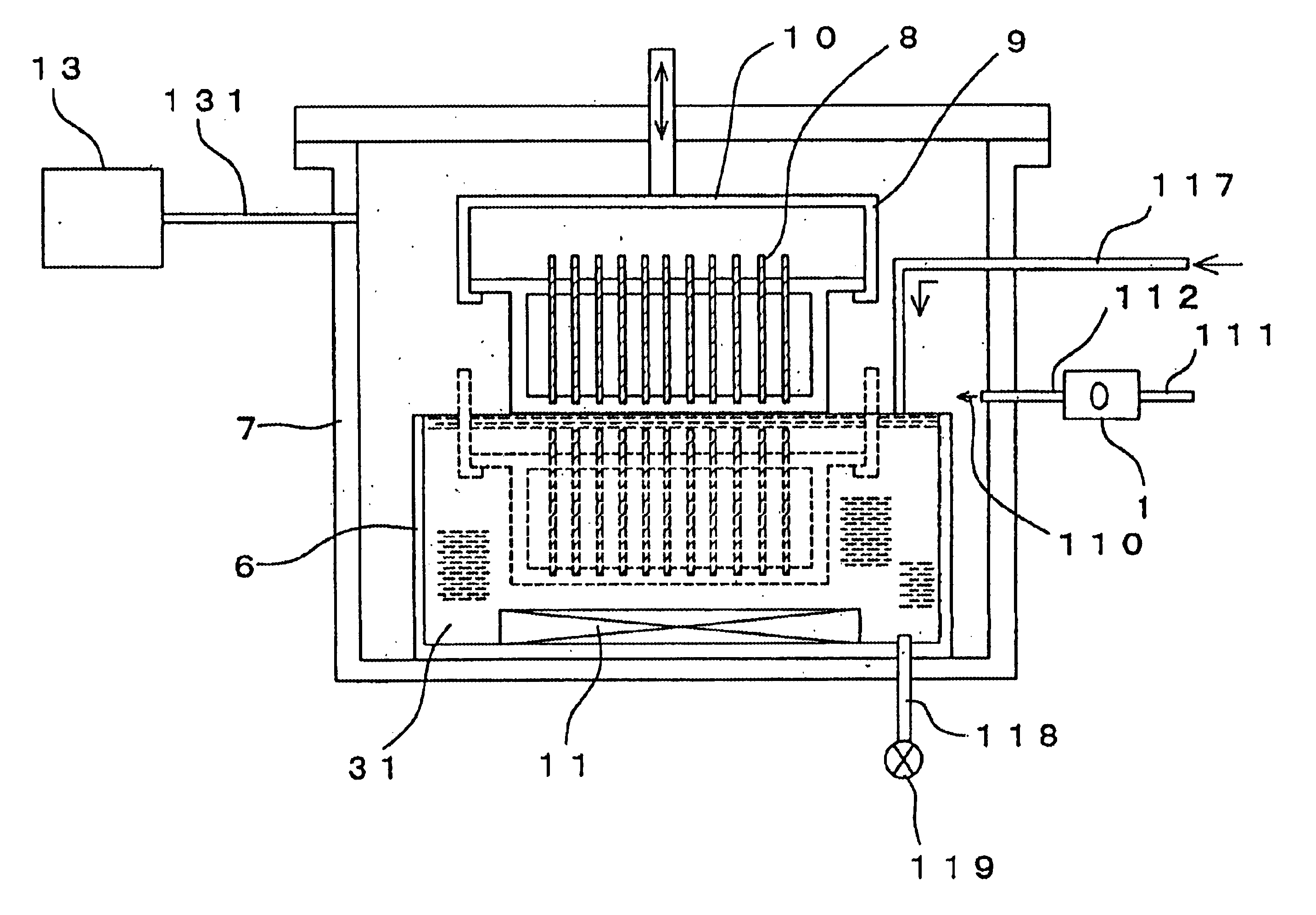
The embodiment 1 relates to a method of removing a photoresist film using an apparatus for removing a photoresist film (A1, FIG. 1) as the second aspect of the invention.
In the present application, the photoresist film to be removed may include either a film formed from a photoresist material containing an organic polymer compound, which the photoresist material is used in any processes of manufacturing semiconductor devices, a film decomposed by heating, a film of which the surface is modified by heating or heavy doping, or a film having a surface on which an inorganic substance is deposited in an etching process.
The substrate of which the surface has the photoresist film may include silicon wafer, a glass substrate for a liquid crystal display device, a glass-reinforced epoxy substrate used for producing a printed-circuit, and the like, but is not particularly limited thereto as long as it may be any one commonly used in the manufacture of semiconductor devices.
Apparatus
An apparat...
embodiment 2
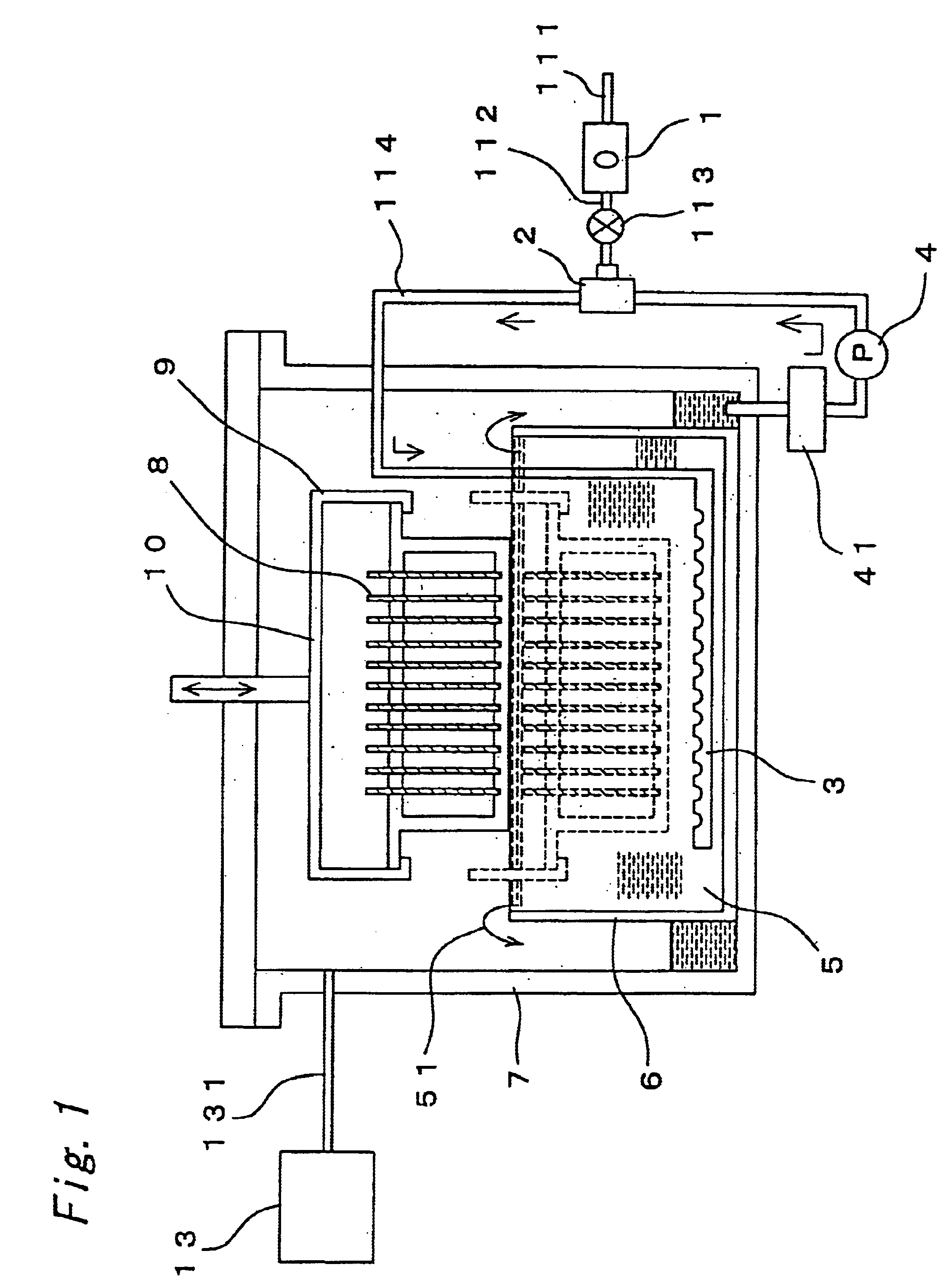
The above embodiment 1 illustrates the method and the apparatus of moving the substrate itself in order to change the relative position of the surface of the substrate and the liquid surface of the solution. The present invention, however, also provides another method and apparatus which can change the liquid surface of the photoresist film removing solution to control the relative position. FIG. 4 shows an apparatus which is able to change the liquid surface of the solution to control the relative position.
The apparatus (A2) shown in FIG. 4 has a constitution typically similar to that of the apparatus (A1) shown in FIG. 1 (that is, the raw gas is a oxygen-containing gas, and any of the photoresist film removing solution described in embodiment 1 may be used). In the apparatus (A2) of embodiment 2, however, it is not essential to move the substrate 8 vertically using the cassette carrier unit 10 in the sealed container 7. An automatically operated valve 61 is equipped with the react...
embodiment 3
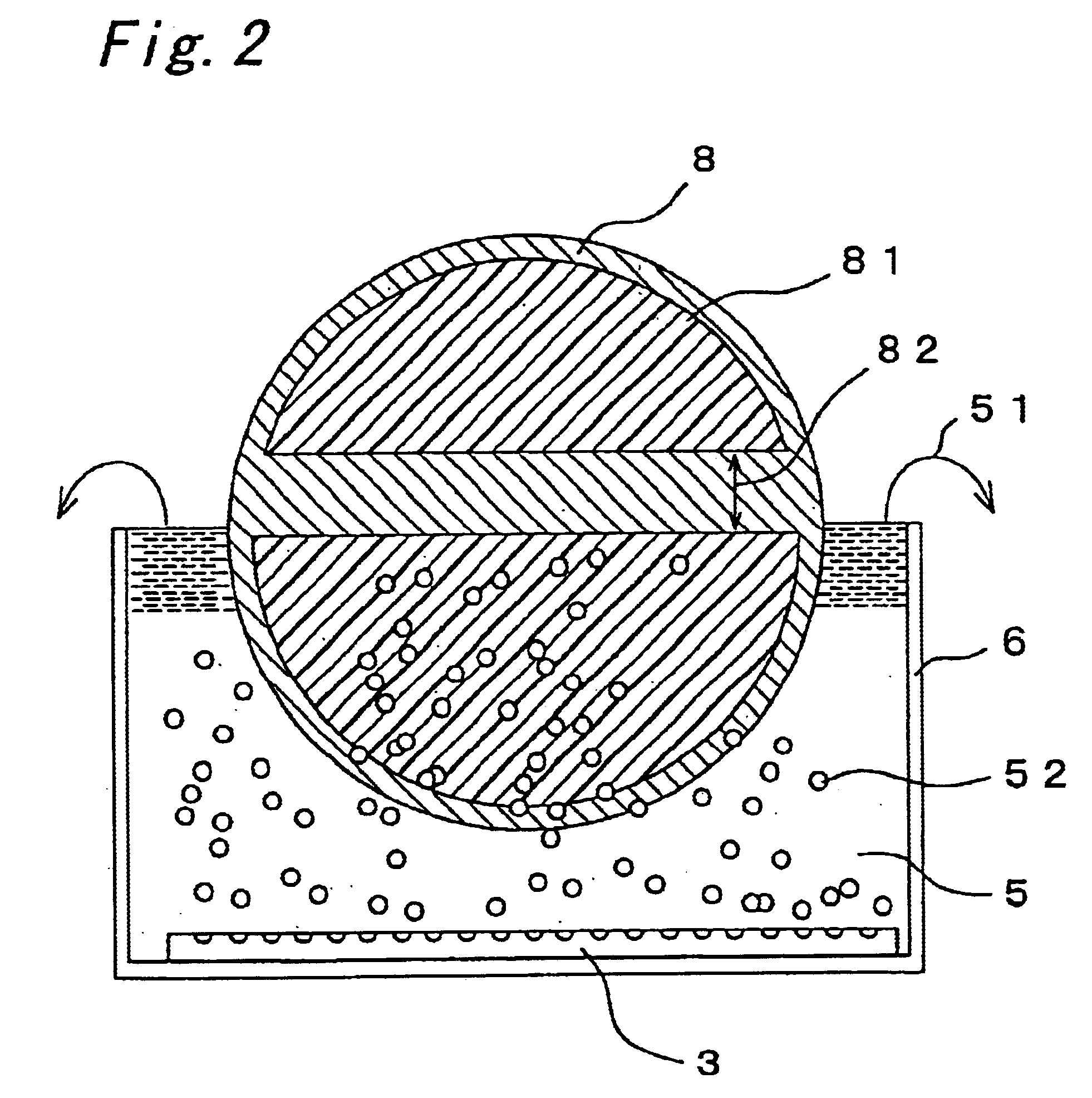
The present invention also provides a different method and apparatus other than those described above embodiments 1 and 2, further including an ultrasound generating means in the apparatus, and applying ultrasonic vibration to the photoresist film removing solution containing the ozonized gas and the substrate using the ultrasound generating means, in order to improve the efficiency of the process capacity.
FIG. 5 illustrates an example of an apparatus of removing a photoresist film (A3) used in this embodiment 3, wherein most of the apparatus may be the same as that described in this embodiment 1, with the exception of an element and a function specifically described).
The ultrasound generating means 71 used in the apparatus (A3) of the embodiment 3 may be one that is well known in the prior art. The ultrasound generating means 71 is laid adjacent to the bottom of the sealed container 7 in FIG. 5, but is not limited thereto. As long as the ultrasonic vibration can be effectively appl...
PUM
| Property | Measurement | Unit |
|---|---|---|
| speed | aaaaa | aaaaa |
| temperature | aaaaa | aaaaa |
| time | aaaaa | aaaaa |
Abstract
Description
Claims
Application Information