Method of making ultra thin oxide formation using selective etchback technique integrated with thin nitride layer for high performance MOSFET

Inactive Publication Date: 2004-07-27
ADVANCED MICRO DEVICES INC
View PDF14 Cites 7 Cited by
  • Summary
  • Abstract
  • Description
  • Claims
  • Application Information

AI Technical Summary

Benefits of technology

Advantageously, the dimensions of the silicon dioxide knob can be varied to form a graded channel having a different geometry. The steps are easily performed and one implantation for heavy doping is all that is needed to form the graded junction or doping pattern. The resulting device has a longe

Problems solved by technology

Trapped charge in the gate insulator due to injected hot carriers accumulates over time and can lead to a permanent change in the threshold voltage of the device.
Trapped charge in the gate insulator due to injected hot carriers accumulates over time and can lead to a permanent chang

Method used


Image

  • Method of making ultra thin oxide formation using selective etchback technique integrated with thin nitride layer for high performance MOSFET
  • Method of making ultra thin oxide formation using selective etchback technique integrated with thin nitride layer for high performance MOSFET
  • Method of making ultra thin oxide formation using selective etchback technique integrated with thin nitride layer for high performance MOSFET

Examples


Embodiment Construction

In the following detailed description of the preferred embodiments, reference is made to the accompanying drawings which form a part hereof, and in which are shown by way of illustration specific embodiments in which the invention may be practiced. It is to be understood that other embodiments may be utilized and structural changes may be made without departing from the scope of the present invention.

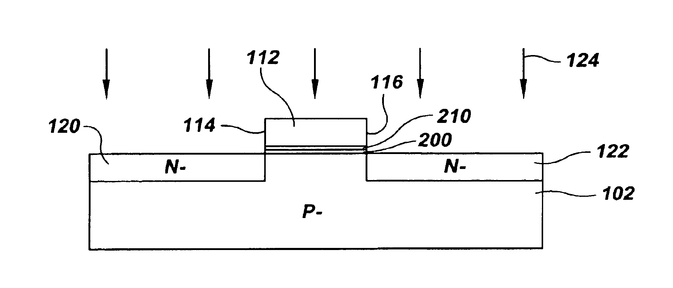
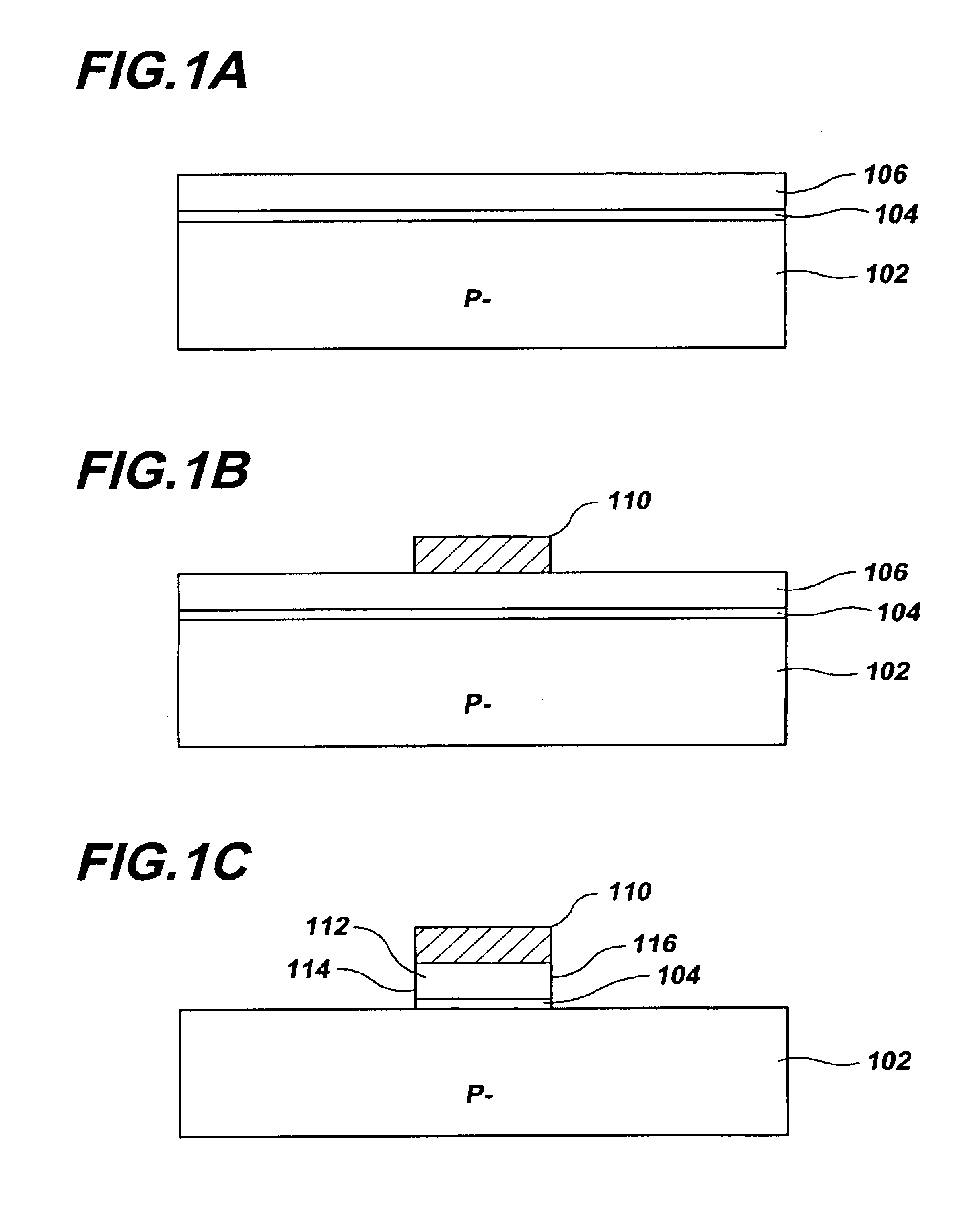
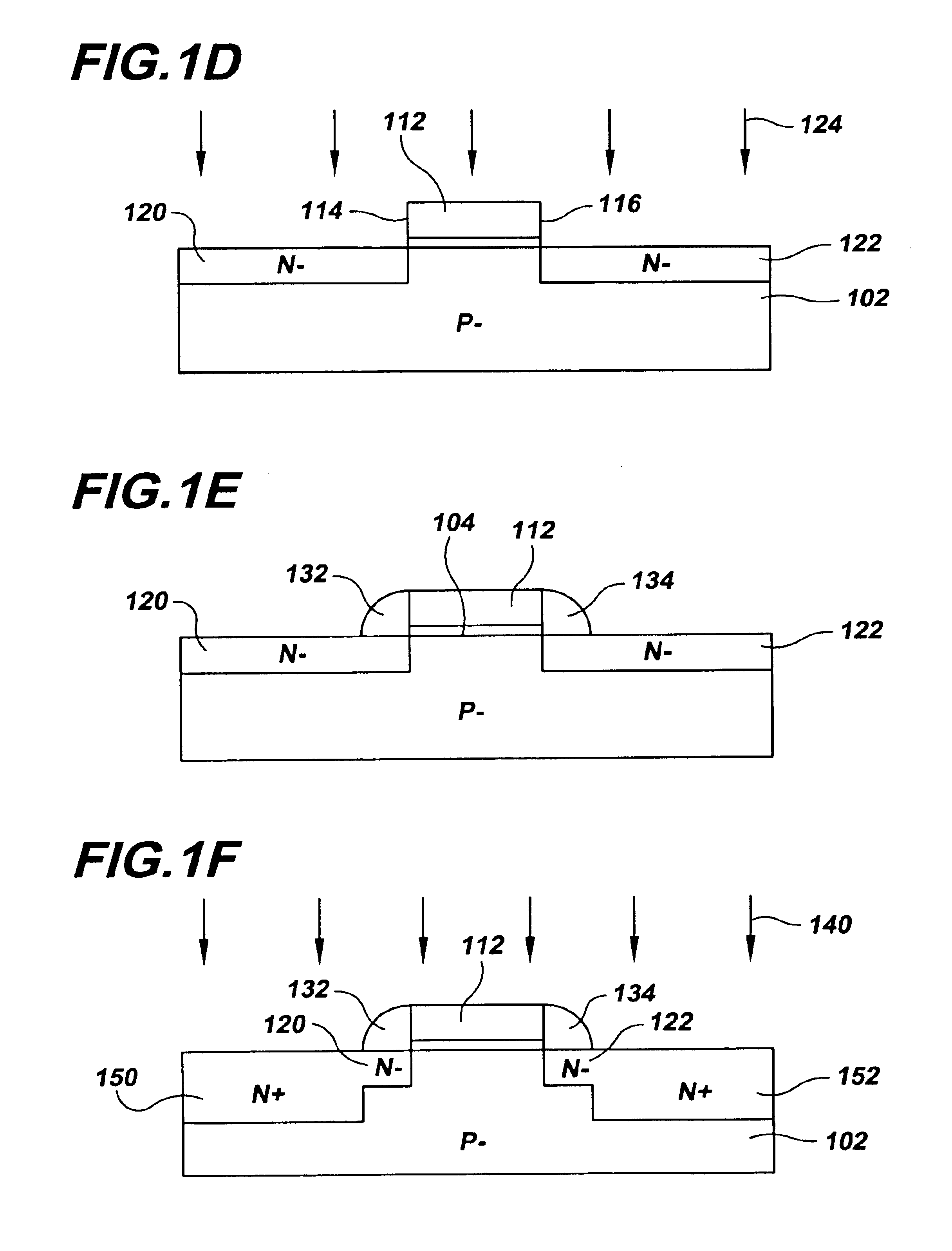
An NMOSFET is described to show the most common method for forming a transistor device with a graded source and drain. The NMOSFET has a silicon dioxide gate oxide with a graded doped drain and source. In FIG. 1A, silicon substrate 102 suitable for integrated circuit manufacture includes P-type epitaxial layer with a boron background concentration on the order of 1.times.10.sup.16 atoms / cm.sup.3, a orientation and a resistivity of 12 ohm-cm. Preferably, the epitaxial surface layer is disposed on a P+ base layer (not shown) and includes a planar top surface. Gate oxide 104, composed of s...


PUM


Abstract

A semiconductor device having gate oxide with a first thickness and a second thickness is formed by initially implanting a portion of the gate area of the semiconductor substrate with nitrogen ions and then forming a gate oxide on the gate area. Preferably the gate oxide is grown by exposing the gate area to an environment of oxygen. A nitrogen implant inhibits the rate of SiO.sub.2 growth in an oxygen environment. Therefore, the portion of the gate area with implanted nitrogen atoms will grow or form a layer of gate oxide, such as SiO.sub.2, which is thinner than the portion of the gate area less heavily implanted or not implanted with nitrogen atoms. The gate oxide layer could be deposited rather than growing the gate oxide layer. After forming the gate oxide layer, polysilicon is deposited onto the gate oxide. The semiconductor substrate can then be implanted to form doped drain and source regions. Spacers can then be placed over the drain and source regions and adjacent the ends of the sidewalls of the gate.

Description

FIELD OF THE INVENTIONThe present invention relates generally to integrated circuit manufacturing and more particularly to forming insulated gate field effect transistors.BACKGROUND OF THE INVENTIONAn insulated-gate field-effect transistor (IGFET), such as a metal-oxide semiconductor field-effect transistor (MOSFET), uses a gate to control an underlying surface channel joining a source and a drain. The channel, source and drain are located in a semiconductor substrate, with the source and drain being doped oppositely to the substrate. The gate is separated from the semiconductor substrate by a thin insulating layer such as a gate oxide. Currently, the gate oxide is formed having a substantially uniform thickness. The operation of the IGFET involves application of an input voltage to the gate, which sets up a transverse electric field in the channel in order to modulate the longitudinal conductance of the channel.In typical IGFET processing, the source and drain are formed by introdu...

Claims


Application Information

Patent Timeline
IPC IPC(8): H01L21/02H01L21/28H01L29/40H01L29/51H01L21/314
CPCH01L21/28185H01L21/28202H01L21/28211H01L29/513H01L29/518H01L21/3144H01L21/022
Inventor GARDNER, MARK I.ALLEN, MICHAELFULFORD, H. JAMES
Owner ADVANCED MICRO DEVICES INC
Why Eureka
Try Eureka