
Formation of nanoscale wires

a nano-scale wire and wire technology, applied in the direction of polycrystalline material growth, crystal growth process, chemically reactive gas, etc., can solve the problems of irregular shape and size, difficult to achieve, and wire-like structur

Inactive Publication Date: 2004-08-10
HEWLETT-PACKARD ENTERPRISE DEV LP
View PDF6 Cites 135 Cited by
  • Summary
  • Abstract
  • Description
  • Claims
  • Application Information

AI Technical Summary

Benefits of technology

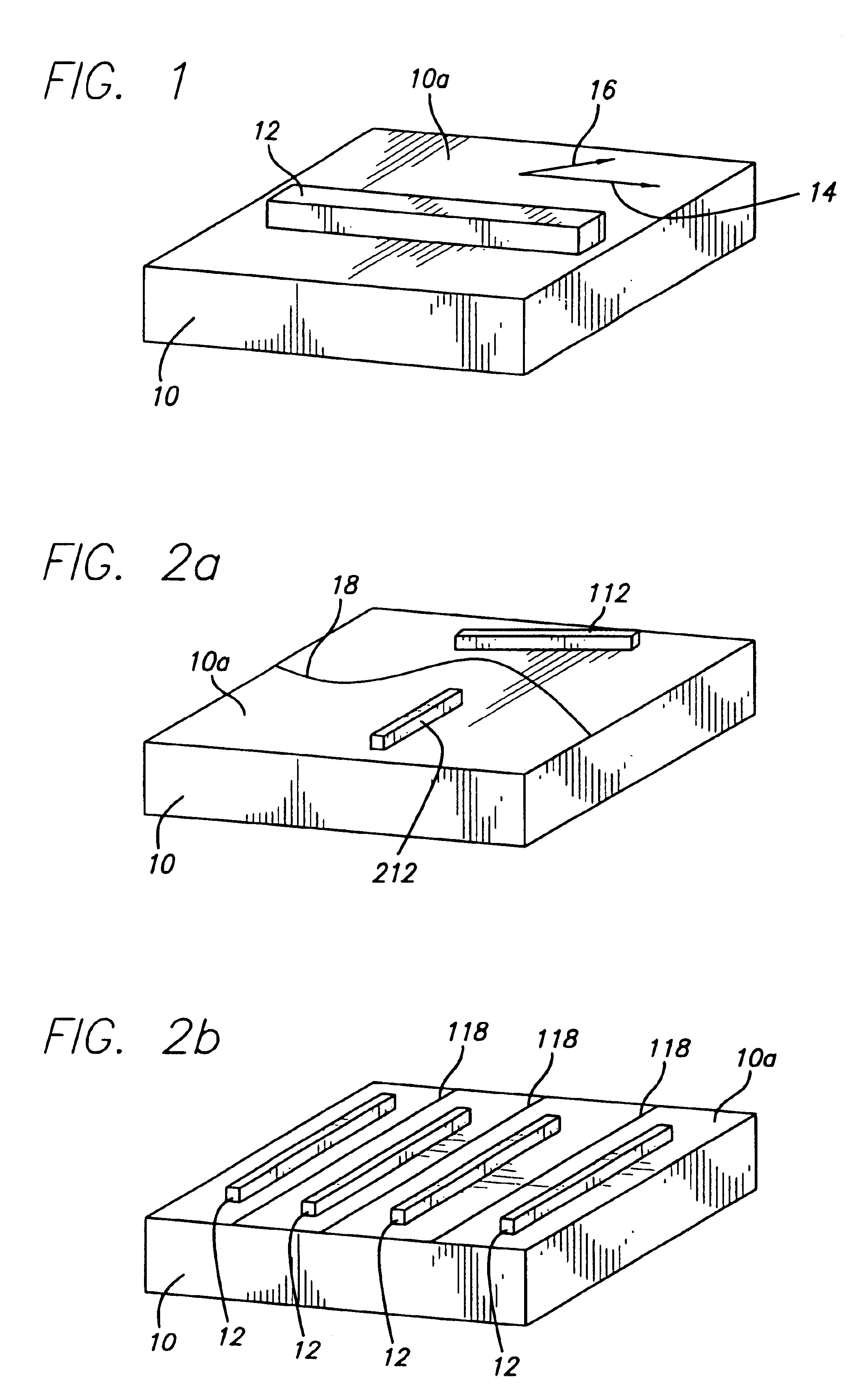
The present invention provides a means to form essentially one-dimensional crystalline nanowires with widths and heights at the nanometer scale, and lengths at the micrometer scale, which are aligned along certain crystallographic directions with high crystal quality. Further, the present invention avoids traditional lithography methods, minimizes environmental toxic chemicals usage, simplifies the manufacturing processes, and allows the formation of high-quality one-dimensional nanowires over large areas.

Problems solved by technology

However, the formation of robust "one"-dimensional nanowires with a width less than 10 nm has been a major goal that has proven difficult to achieve by either epitaxial growth or lithographic processing.
However, they often produce wire-like structures that meander along with the steps, are terminated by single steps, have irregular shapes and sizes, and / or are not robust.
These lattice-mismatched systems will thus limit the lateral growth in all directions on the substrate surface and produce strained islands.
Such masks are ordinarily difficult to make on a nanoscale, due partly to the extremely small dimensions and due partly to the need to employ materials having differential etch rates.

Method used


Image

  • Formation of nanoscale wires
  • Formation of nanoscale wires
  • Formation of nanoscale wires

Examples


example 1

Growth of ErSi.sub.2 on Si.

The following example demonstrates that by utilizing an epitaxial overlayer that has a carefully chosen lattice mismatch to complement the host substrate, in this case erbium disilicide (ErSi.sub.2) on Si(001), it is possible to grow nanowires. Due to its high conductivity (2.9.times.10.sup.4 (.OMEGA.cm).sup.-1) and low Schottky barrier to n-type Si, ErSi.sub.2 thin films grown on Si substrates have been studied extensively. These studies involved continuous thin films on Si(001) that were several nanometers thick, and they revealed oriented crystallites with a hexagonal AlB.sub.2 -type crystal structure that were thermodynamically stable in contact with Si below 800.degree. C. The [0001] axis of the ErSi.sub.2 was oriented along a (110) axis of the Si(001) substrate, and the [1120] of the ErSi.sub.2 was oriented along the perpendicular (110) axis, with lattice mismatches of +6.5% and -1.3%, respectively, which nearly satisfies the proposed growth conditio...

example 2

Growth of EtSi.sub.2, ScSi.sub.2, DvSi.sub.2, and GdSi.sub.2 on Si and Their Comparison.

In the following experiments, device quality "flat" Si(001) substrates were prepared as in Example 1.

As measured from STM images, the average terrace widths along [110].sub.Si and [110].sub.Si were 57.8 nm and 21.3 nm, respectively, implying that the normal direction of the surface of the Si substrate used in these experiments was misoriented from [001].sub.Si toward [120].sub.Si by about 0.4.degree..

The final state of the nanowires was influenced by their growth conditions, such as deposition and annealing temperature, deposition rate, coverage of deposited atoms, and annealing time. The physical properties of Sc, Er, Dy, and Gd are similar (e.g., their melting points are 1539.degree. C., 1522.degree. C., 1409.degree. C., and 1314.degree. C. respectively), and the experimentally-determined growth conditions for producing dislocation-free nanowires are also very close. The optimum substrate tempe...

example 3

Patterning Silicon to Form Silicon Nanowires.

ErSi.sub.2 nanowires, about 1 nm thick, were grown on a Si(001) substrate, as described in Example 1. FIG. 6a is a scanning electron microscope (SEM) image of the ErSi.sub.2 self-assembled nanowires grown on the Si substrate. The ErSi.sub.2 lines appear to be weaker in FIG. 6a than the Si lines in FIG. 6b, due to the fact that the ErSi.sub.2 wires are less than 1 mm and their interaction with the e-beam in the SEM are very weak.

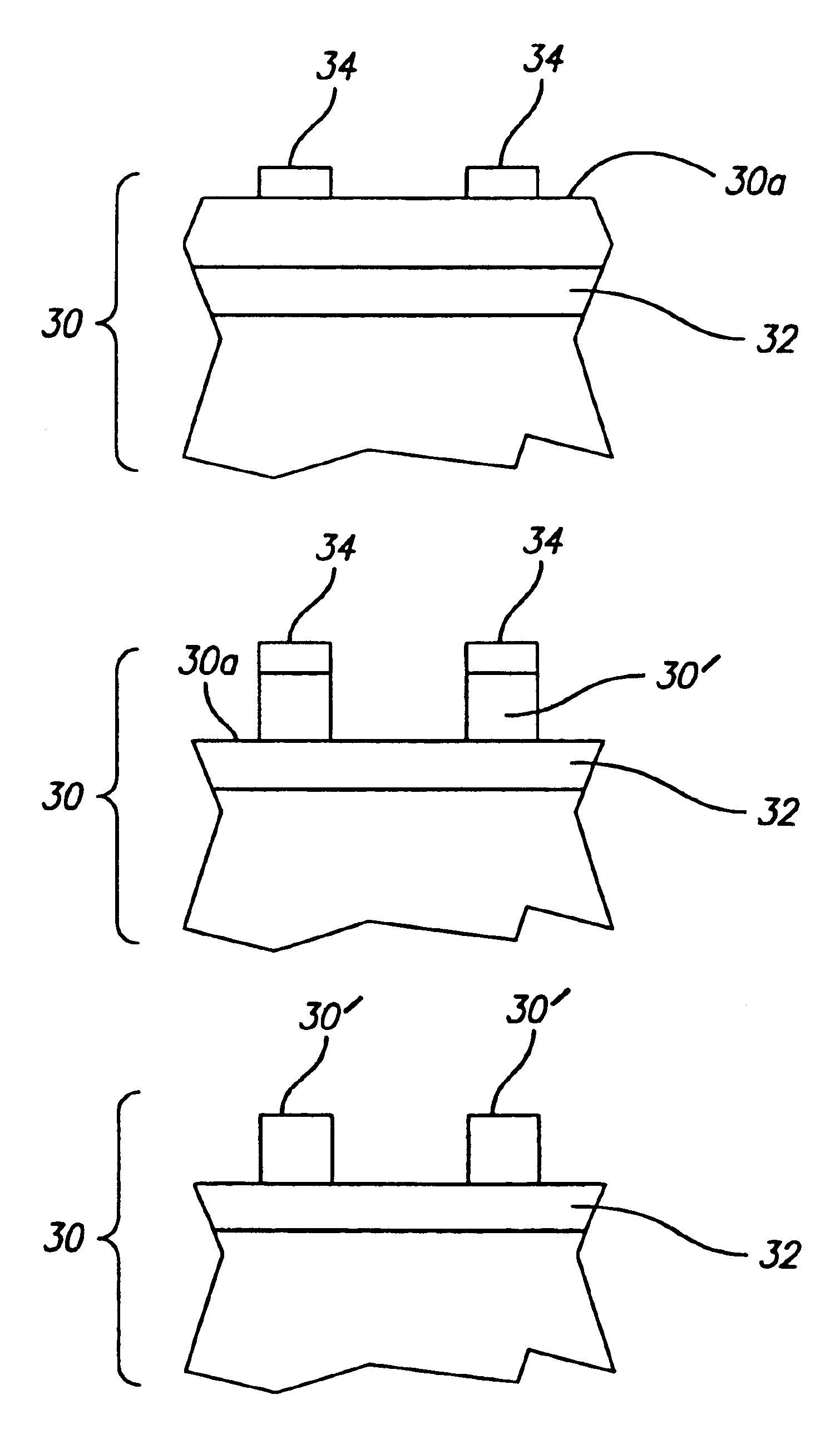
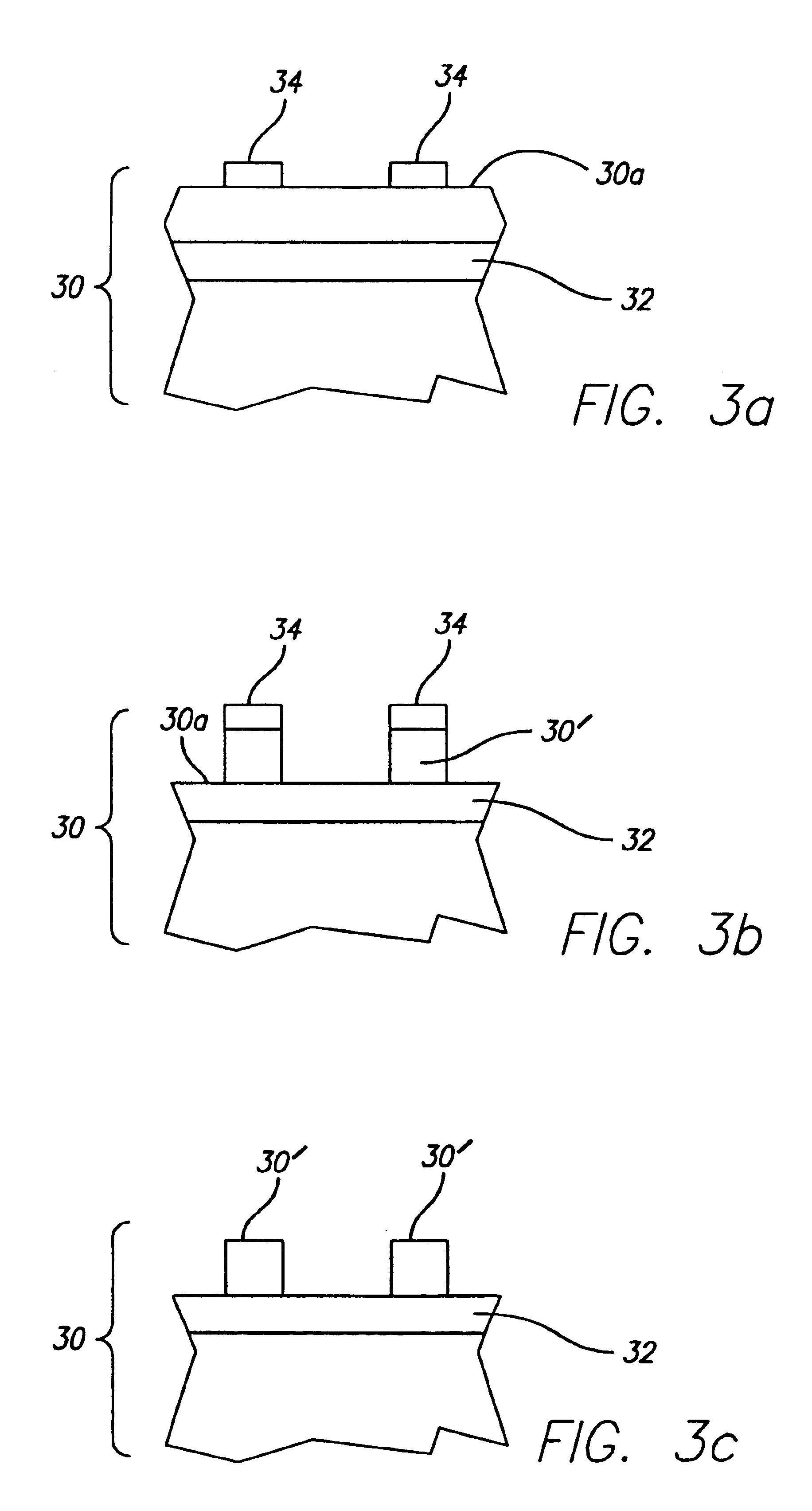
Using the ErSi.sub.2 nanowires as a mask, the silicon was anisotropically etched away in the area without the coverage of the ErSi.sub.2 nanowires. The etching was carried out by RIE for 5 minutes in CF.sub.4, SF.sub.6, and Ar gases with their flowing rates as CF.sub.4 :SF.sub.6 :Ar=25 sccm:125 sccm:60 sccm, at a pressure of 50 mTorr and a power of 100 W. ErSi.sub.2 was subsequently removed from the tops of the Si nanowires, using HF. The resulting silicon nanowires were about 9 nm in height. FIG. 6b is an SEM imag...


PUM

PropertyMeasurementUnit
Thicknessaaaaaaaaaa
Angleaaaaaaaaaa
Angleaaaaaaaaaa

Abstract

Self-organized, or self-assembled, nanowires of a first composition may be used as an etching mask for fabrication of nanowires of a second composition. The method for forming such nanowires comprises: (a) providing an etchable layer of the second composition and having a buried insulating layer beneath a major surface thereof; (b) growing self-assembled nanowires on the surface of the etchable layer; and (c) etching the etchable layer anisotropically down to the insulating layer, using the self-assembled nanowires as a mask. The self-assembled nanowires may be removed or left. In either event, nanowires of the second composition are formed. The method enables the formation of one-dimensional crystalline nanowires with widths and heights at the nanometer scale, and lengths at the micrometer scale, which are aligned along certain crystallographic directions with high crystal quality. Further, the method of the present invention avoids traditional lithography methods, minimizes environmental toxic chemicals usage, simplifies the manufacturing processes, and allows the formation of high-quality one-dimensional nanowires over large areas.

Description

The present invention is related generally to electronic devices whose functional scales are measured in nanometers, and, more particularly, to forming one-dimensional epitaxial crystals with widths and heights at the nanometer scale.The synthesis of artificial low-dimensional structures to confine electrons has been a topic of scientific and technical interest for decades. Epitaxial deposition techniques have made possible the growth of two-dimensional quantum wells as thin as one atomic layer and "zero"-dimensional islands as small as a few nanometers. However, the formation of robust "one"-dimensional nanowires with a width less than 10 nm has been a major goal that has proven difficult to achieve by either epitaxial growth or lithographic processing. Various "self-assembly" techniques, in which structures form spontaneously under kinetic or thermodynamic control, have been used to grow wire-like structures directly on a semiconductor surface. Previous demonstrations include deco...

Claims


Application Information

Patent Timeline
IPC IPC(8): C30B25/02C30B23/02
CPCC30B23/02C30B25/02C30B29/605Y10S977/888
Inventor CHEN, YONGOHLBERG, DOUGLAS A. A.KAMINS, THEODORE I.WILLIAMS, R. STANLEY
Owner HEWLETT-PACKARD ENTERPRISE DEV LP
Learn More