

Ultraviolet and vacuum ultraviolet transparent polymer compositions and their uses
a technology of ultraviolet light and polymer composition, applied in the field of ultraviolet and vacuum ultraviolet light transparent polymer composition, can solve the problems of affecting the transmission range of the approach to increase affecting the effect of the pellicle, and affecting the transmission range of the pellicl
- Summary
- Abstract
- Description
- Claims
- Application Information
AI Technical Summary
Problems solved by technology
Method used
Image

Examples
examples
Many of the polymers tested were obtained as commercial samples.
Teflon.RTM. AF 1200: DuPont, Wilmington, Del.
Teflon.RTM. AF 1600: DuPont
Teflon.RTM. AF 2400: DuPont
Cytop.TM.: Asahi Glass, poly[perfluoro(butenyl vinyl ether)]
.about.1:1 Poly(hexafluoropropylene:tetrafluoroethylene) was made by the procedure described in U.S. Pat. No. 5,478,905, Dec. 26, 1995.
Many of remaining polymer compositions are known to the art and were prepared by standard methods. Typically autoclaves were loaded with monomer, solvent and initiator and heated to start polymerization. Most polymerizations were initiated using hexafluoropropylene oxide dimer peroxide 1 (DP) at ambient temperatures.
CF.sub.3 CF.sub.2 CF.sub.2 OCF(CF.sub.3)(C.dbd.O)OO(C.dbd.O)CF(CF.sub.3)OCF.sub.2 CF.sub.2 CF.sub.3 1, DP
DP was prepared and used as a 0.05 to 0.2 molar solution in solvents such as Vertrel.TM. XF (CF.sub.3 CFHCFHCF.sub.2 CF.sub.3) or 3M's Performance Fluid PF-5080 (largely perfluorooctane). DP can be made conveniently ...
example 1
PDD / TFE
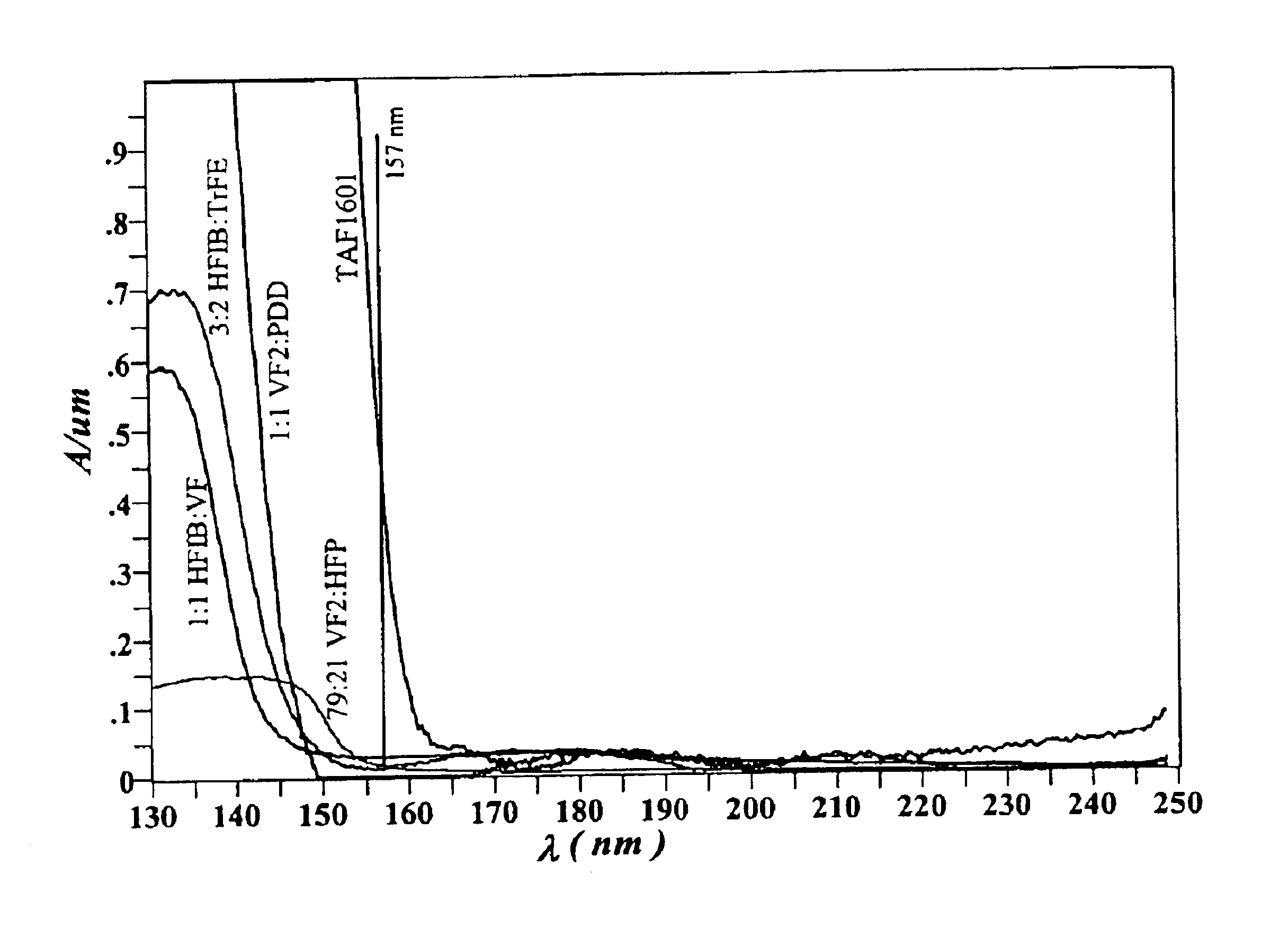
Solutions of Teflon.RTM. AF 1200, 1601, and 2400 were spin coated at spin speeds of 6000 rpm onto CaF.sub.2 substrates to produce polymer films of 4066 angstroms, 3323 angstroms and 2133 angstroms thicknesses respectively. VUV absorbance measurements were then used to determine the absorbance per micron.
The absorbance in units of inverse microns for Teflon.RTM. AF 1200 versus wavelength lambda (.lambda.) in units of nanometers is shown in FIG. 7 for sample 8. The 157 nm absorbance / micron determined is 0.64 / micron. The 193 nm absorbance / micron determined is 0.004 / micron. The 248 nm absorbance / micron determined is -0.001 / micron.
The absorbance in units of inverse microns for Teflon.RTM. AF 1601 versus wavelength lambda (.lambda.) in units of nanometers is shown in FIG. 7 for Sample 7a The 157 nm absorbance / micron determined is 0.42 / micron. The 193 nm absorbance / micron determined is 0.02 / micron. The 248 nm absorbance / micron determined is 0.01 / micron.
The absorbance in units of inv...
example 2
HFIB / TrFE
Preparation of 1:1 Poly(hexafluoroisobutylene:Trifluoroethylene)
A 75 ml stainless steel autoclave chilled to <-20.degree. C. was loaded with 25 ml of CCl.sub.2 FCF.sub.2 Cl and 5 ml of .about.0.17 M DP in Vertrel.TM. XF. The autoclave was cooled, evacuated, and further loaded with 10 g of trifluoroethylene and 20 g of hexafluoroisobutylene. The reaction mixture was shaken overnight at ambient temperatures (28 to 33.degree. C.), removed from the autoclave, and evaporated down to a glassy film that was further dried for 72 hours in a 75.degree. C. vacuum oven. There was obtained 3.33 g of white solid. A solution was made by rolling 3.24 g of this polymer with 6.99 g of 1-methoxy-2-propanol acetate (PGMEA). This solution was mixed with 0.2 g of chromatographic silica gel and 0.2 g of decolorizing carbon and then passed first through a 0.45.mu. glass microfiber syringe filter (Whatman, Autovial.TM.) and then through a 0.45.mu. PTFE membrane syringe filter (Whatman, Autovial.TM....
PUM
| Property | Measurement | Unit |
|---|---|---|
| wavelength range | aaaaa | aaaaa |
| molar ratio | aaaaa | aaaaa |
| wavelength region | aaaaa | aaaaa |
Abstract
Description
Claims
Application Information