

High gain integrated antenna and devices therefrom
- Summary
- Abstract
- Description
- Claims
- Application Information
AI Technical Summary
Benefits of technology
Problems solved by technology
Method used
Image

Examples
examples
[0042]It should be understood that the examples and embodiments described herein are for illustrative purposes only and that various modifications or changes in light thereof will be suggested to persons skilled in the art and are to be included within the spirit and purview of this application. The invention can take other specific forms without departing from the spirit or essential attributes thereof.
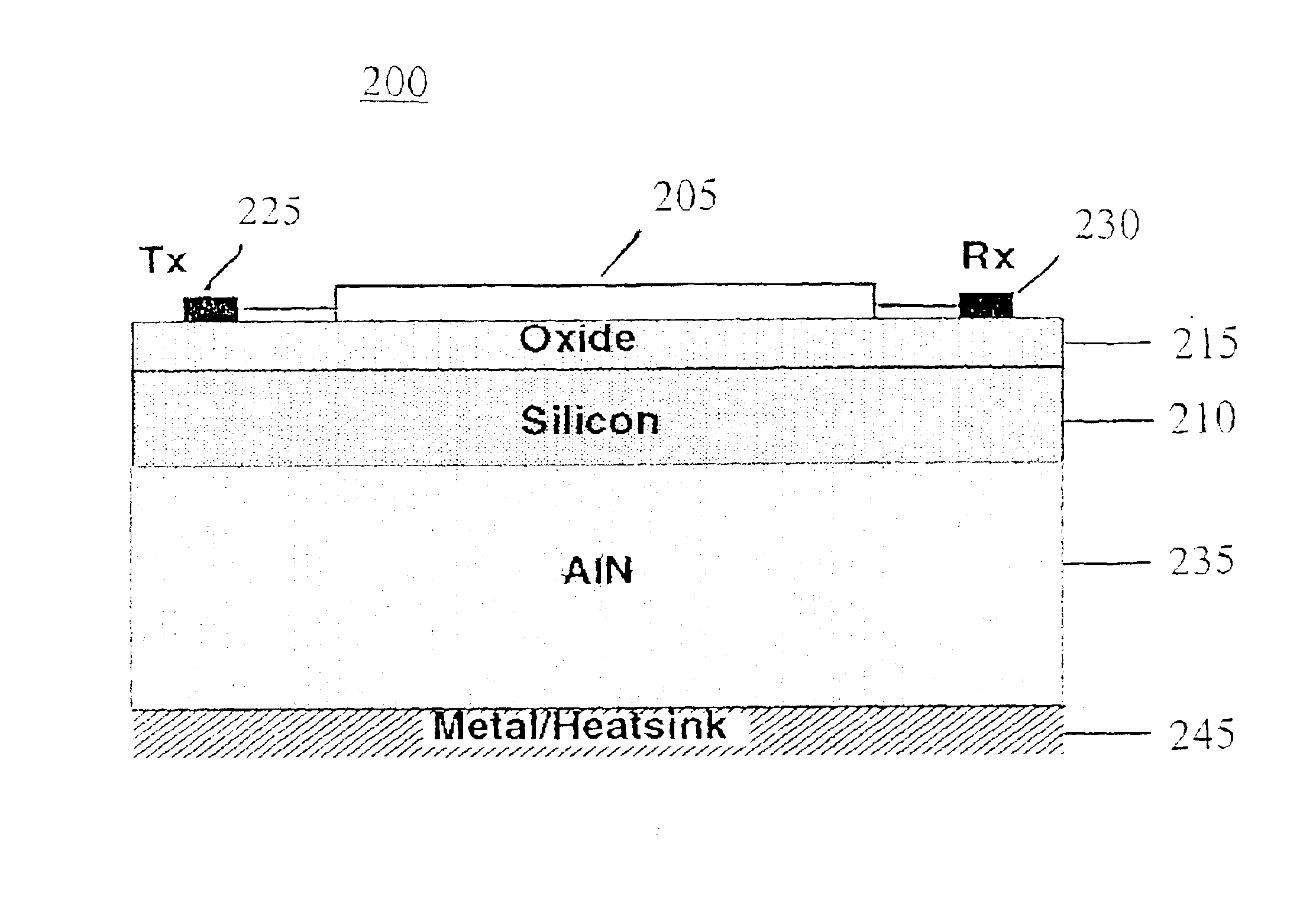
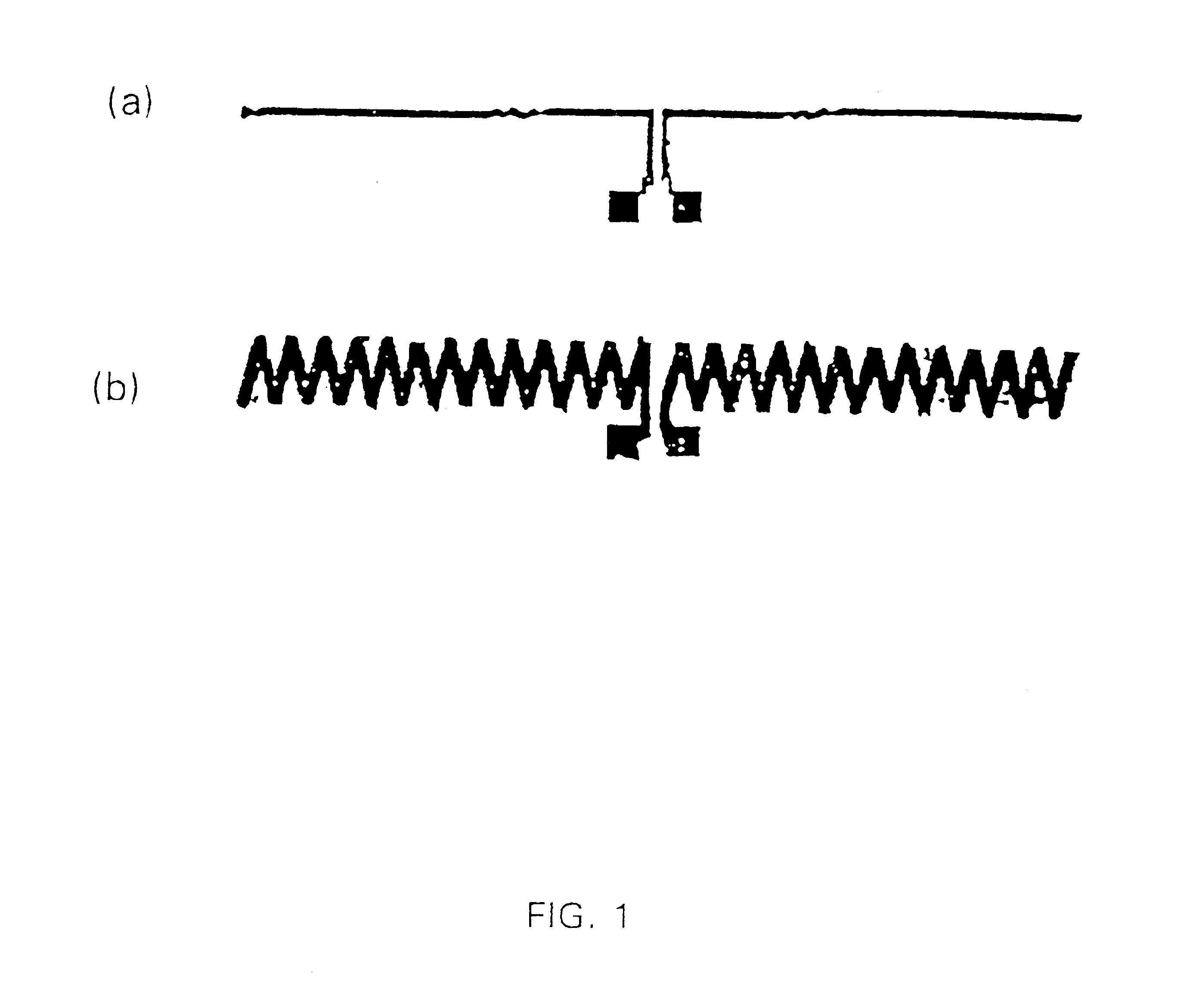
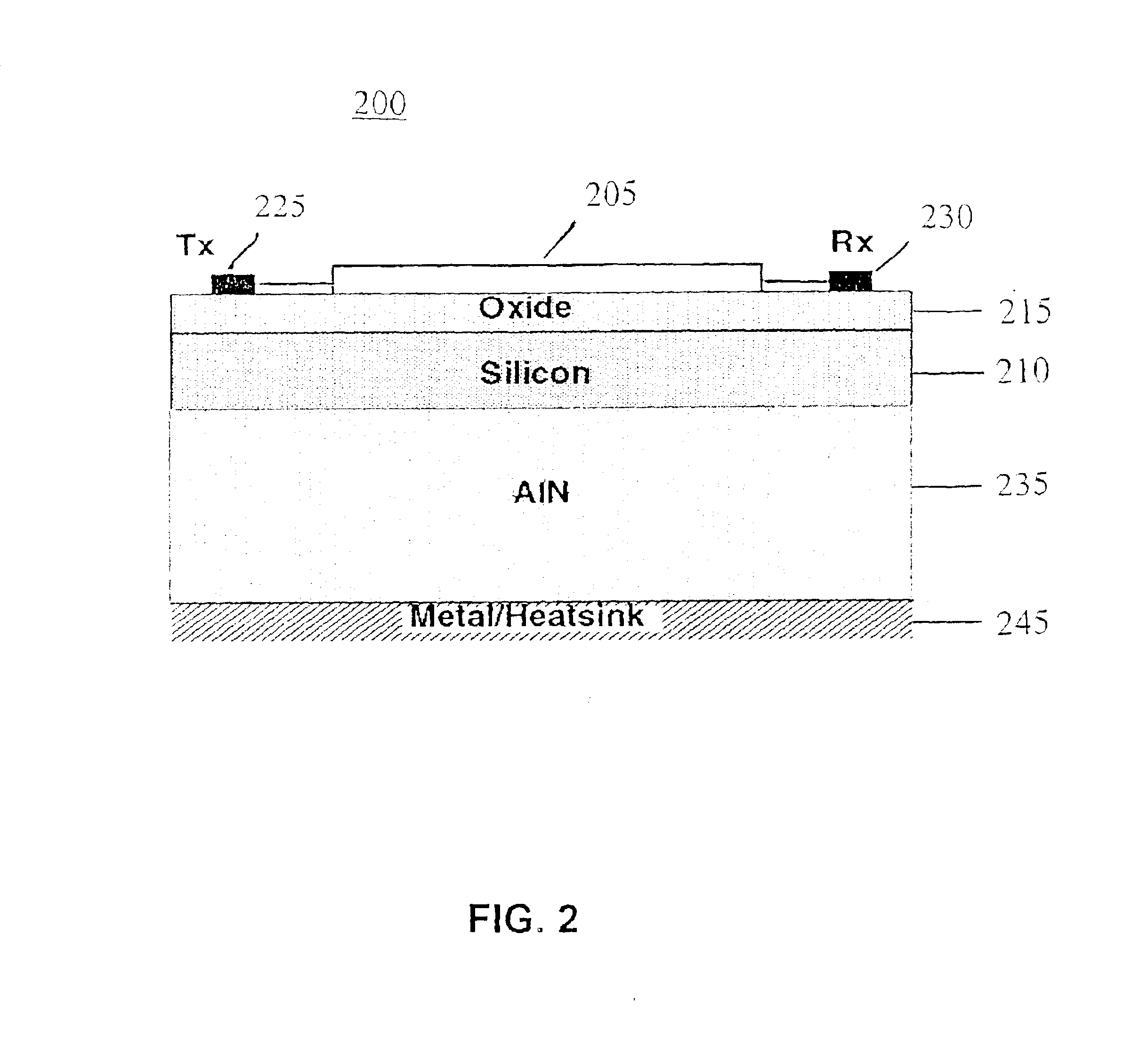
[0043]To evaluate the impact of a propagating layer disposed underneath a silicon substrate for lessening the influence from a lossy metallic heat sink, linear or zigzag dipole antenna pairs (FIGS. 1(a) and (b)) were each fabricated using a single metal level process without a passivation layer and disposed on a silicon wafer. The antennas were 2 mm long, and the thickness and width of the metal lines were 2 μm and 10 μm, respectively.
[0044]As noted above, FIG. 2 shows transmit 225 and receive 230 dipole antennas disposed on a silicon dioxide 215 covered silicon wafer 210, where a Al...
PUM
 Abstract
Description
Claims
Application Information