Display device

a display device and liquid crystal technology, applied in static indicating devices, instruments, cross-talk/noise/interference reduction, etc., can solve the problems of so-called “narrowing of frames” becoming extremely difficult, and the problem becomes all the more remarkable, so as to reduce the outer dimension of the liquid crystal display device, reduce the production cost, and simplify the construction.

Inactive Publication Date: 2005-01-11
PANASONIC LIQUID CRYSTAL DISPLAY CO LTD +1
View PDF6 Cites 23 Cited by
  • Summary
  • Abstract
  • Description
  • Claims
  • Application Information

AI Technical Summary

Benefits of technology

When the lines are extended outside the outer shape of the product of the liquid crystal panel while passing below the body of the driver chip, the common lines can be disposed at a cutting / removing portion outside the product. In this case, the common lines can be cut off simultaneously with the cutting process of the substrate (lower substrate: glass) of the liquid crystal panel. In consequence, the conventional cutting process by using laser can be omitted, and the production cost can be lowered.18) When the lines for the clock, data and gray scale voltage are wired on the lower substrate (TFT substrate), it is fundamentally only the power supply lines that must be wired on the flexible printed substrate. In any case, the number of lines is only a few. Therefore, even when the flexible printed substrate FPC is not folded to the back of the liquid crystal panel as has been necessary in the conventional system, the required portion is only the width of the compression-bonding portion to the liquid crystal panel. In this case, the construction can be simplified and the outer dimension of the liquid crystal display device can be reduced. Because the assembly work can be simplified, the cost of production can be reduced.19) In the case 18) described above, when the back of the compression-bonding portion of the flexible printed substrate FPC to the liquid crystal panel is utilized for wiring, design of the flexible printed substrate FPC becomes easier and the cost can be lowered.20) The flexible printed substrate described above basically has a straight shape (simple straight shape) the width of which is only the width of the compression-bonding portion, but a small number of electronic components such as a chip capacitor must be mounted in many cases to this portion. In this case, the electronic components become the obstacle for compression-bonding of FPC. Therefore, the flexible printed substrate FBC is provided with a portion that protrudes into the arrangement gap between the drivers, and the electronic components can be mounted to this protruding portion without any problem.
Furthermore, the present invention omits the flexible printed substrate FPC, that has been used in the past on the gate side, by forming the data lines and the power supply lines on the gate driver side into a substrate shape. The present invention thus decreases the number of components and simplifies the assembly work. The present invention uses a single-layered flexible printed substrate FPC having only the power supply lines as FPC on the drain driver side, and thus simplifies the construction of the drain driver side FPC. Consequently, the present invention can reduce the number of components and the number of process steps of the liquid crystal display device, and can reduce the cost of production.

Problems solved by technology

In either case, the cost is extremely high.
To pattern all these signals and voltages to the side edge of the liquid crystal panel, the periphery of the panel must have a large area, and so-called “narrowing of frame” becomes extremely difficult.
This problem becomes all the more remarkable when resolution (fineness) of the liquid crystal device becomes higher.

Method used


Image

  • Display device
  • Display device
  • Display device

Examples


first embodiment

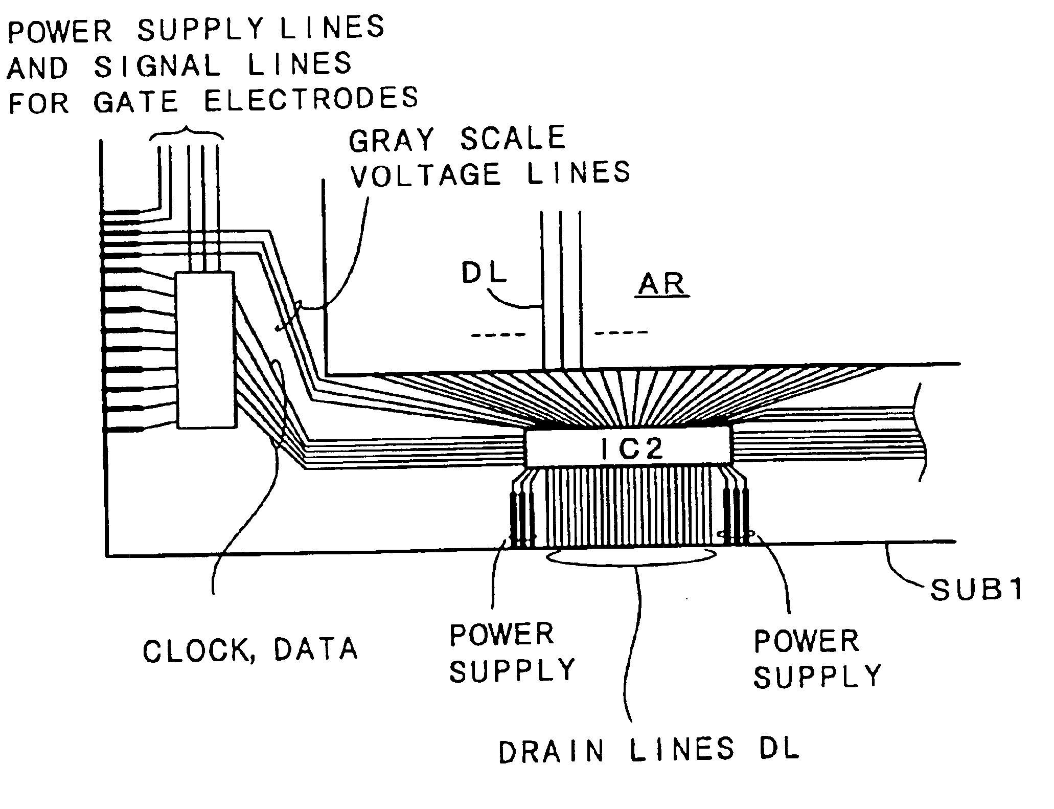
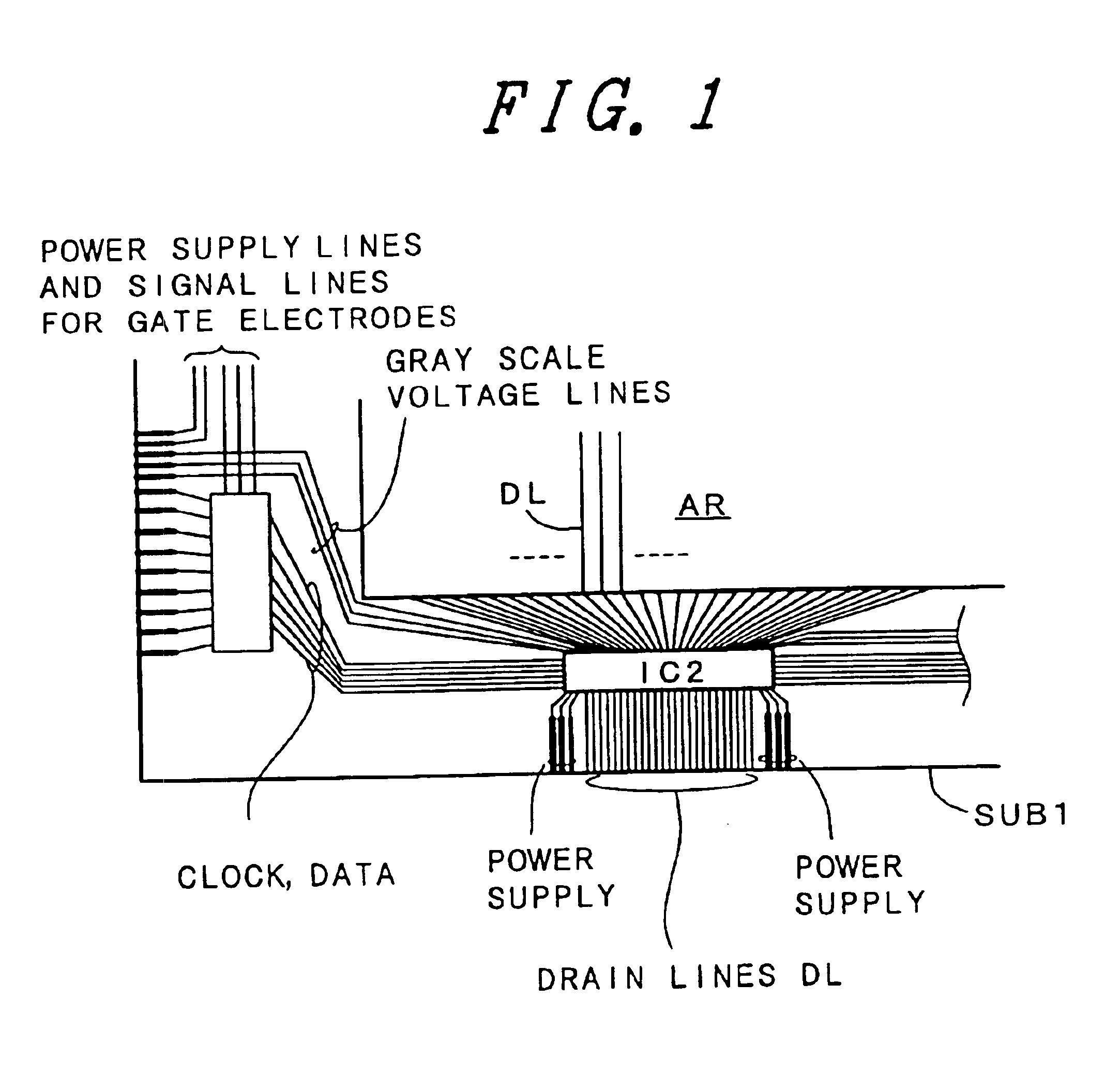
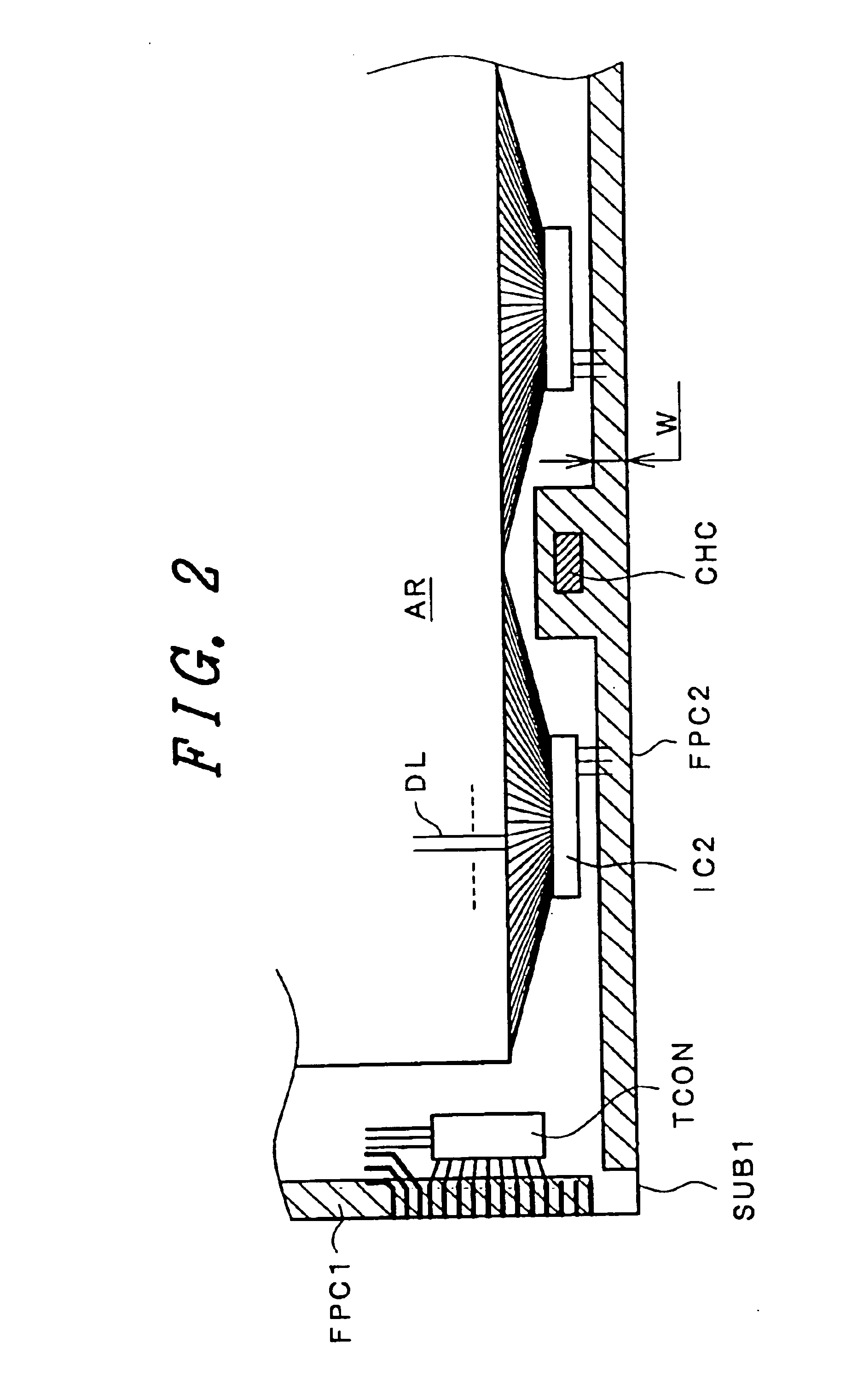
FIG. 1 is a plan view of the principal portions of a liquid crystal panel and is useful for schematically explaining the construction of a liquid crystal display device according to the present invention.

A display area AR occupies substantially the whole area of a lower substrate (glass substrate) constituting the liquid crystal panel. Each drain driver IC2 is mounted to the outer edge of the lower side. (Incidentally, the drain driver IC2 may be mounted to the outer edge of the upper side. Alternatively, odd- and even-numbered drain drivers may be alternately mounted to the outer edges of the upper and lower sides.)

A timing converter TCON that constitutes a display controller integrally having a low voltage differential signal reception circuit is mounted to the outer edge of the left side of FIG. 1. The timing converter TCON is of a so-called LVDS (low voltage differential signal) circuit integration type. However, a known TCON may be used, too.

Though not shown in the drawing, a p...

fourth embodiment

FIG. 12 is a schematic circuit diagram useful for explaining internal circuits of the drain driver in the liquid crystal display device according to the present invention. In this embodiment, a delay device dL is disposed at the output stage of the clock wiring (clock line). This delay device can be constituted by known means that connects a plurality of inverter circuits in series, for example.

FIGS. 13A and 13B are waveform diagrams of the display data signal (FIG. 13B) and the pixel clock signal (FIG. 13A) when the data is acquired by the dual edge system in the construction shown in FIG. 10. As shown in FIGS. 13A and 13B, the setup time tsetup / hold time thold cannot be secured in this case.

FIGS. 14A and 14B show the case where the pixel clock is delayed by the delay device dL (see FIG. 14B) when the display data is acquired by the dual edge system (see FIG. 14B). The drawings also show the waveforms when the wiring resistance connecting the drain drivers is adjusted so as to adju...

seventh embodiment

FIGS. 17A and 17B are explanatory views of the drain driver in the liquid crystal display device according to the present invention. FIG. 17A is a block circuit diagram showing a structural example of internal circuits of the drain driver and FIG. 17B is an explanatory view of the arrangement and operation of the drain driver.

In this embodiment, gates GATa, GATb and GATc are disposed at the display data output and the pixel clock output of the drain driver IC2 as shown in FIG. 17A. These gates GATa, GATb and GATc inhibit the supply of the display data and the clock to the drain driver of the following stage when the drain driver IC2 acquires the display data of its own, and start supplying the display data and the pixel clock to the drain driver of the following stage when the internal register inside its own, that is, the latch circuit (1) LT1, becomes full.

In the construction shown in FIG. 17B, a gate GAT1 to GAT5 comprising the GATa, GATb, GATc shown in FIG. 17A is disposed on th...


PUM

PropertyMeasurementUnit
frequencyaaaaaaaaaa
flexibleaaaaaaaaaa
voltageaaaaaaaaaa

Abstract

In a liquid crystal display comprising a plurality of pixels each of which has an switching element, a plurality of drain drivers and gate drivers for operating the switching elements and the pixels, and a plurality of drain lines and gate lines supplying signals from the drain drivers and the gate drivers to the switching elements being formed on one of a pair of substrates sandwiching a liquid crystal layer, the present invention provides wiring lines formed on the one of a pair of substrates for transferring display data signals and a clock signal between each pair of the plurality of drain drivers adjacent to one another, and provides at least one gate circuit for at least one of the plurality of drain drivers which is controlled by the clock signal and switches the display data signals and the clock signal either (1) to be acquired by the at least one of the plurality of drain drivers or (2) to be transferred to another of the plurality of drain drivers arranged adjacent to the at least one of the plurality of drain drivers. This liquid crystal display device has an advantage, for instance, or of suppressing electromagnetic interference (EMI) to another equipment surrounding the liquid crystal display device, of preventing the display data signals or the clock signal from being distorted in the wiring lines.

Description

BACKGROUND OF THE INVENTION1. Field of the InventionThis invention relates to a liquid crystal display device. More particularly, this invention relates to a liquid crystal display device that simplifies a wiring structure of a flexible printed substrate for supplying driving signals to a driver IC mounted by a flip chip mounting system and reduces a cost by employing a novel signal transmission system.2. Description of the Related ArtLiquid crystal display devices have been wide spread as a display device for various image displaying apparatuses. An active matrix type liquid crystal display device, that has an active cell such as a thin film transistor TFT for each pixel and switches and drives the active cell, applies a liquid crystal driving voltage (gray scale voltage) to a pixel electrode through the active cell. Therefore, this liquid crystal display device is free from cross-talk between the pixels and can conduct multiple gray scale display without employing a specific drivi...

Claims


Application Information

Patent Timeline
Patent Type & Authority Patents(United States)
IPC IPC(8): G09G3/36G09G3/20G02F1/133
CPCG02F1/13452G09G3/2011G09G3/3648G09G3/3688G02F1/13306G09G2310/027G09G2320/0223H05K1/0216H05K1/181G09G2300/0408G02F1/133
Inventor IMAJO, YOSHIHIROIZAWA, TETSUROOHGIICHI, KIMITOSHIOKAWARA, HIROSHIUEDA, SHIROISHIGE, NOBUYUKIKAWAMURA, TETSUYAISHINO, HISASHIKOMORI, FUMIAKI
Owner PANASONIC LIQUID CRYSTAL DISPLAY CO LTD
Why Eureka
Try Eureka