
Optical single sideband transmitter

a transmitter and optical technology, applied in the field of optical single sideband transmitters, can solve the problems of deteriorating optical amplifier performance, reducing pumping efficiency, and increasing costs, so as to prevent the transmitter from becoming complicated and expensive, and not implement a hilbert transform circuit with eas

Inactive Publication Date: 2005-02-01
HITACHI LTD
View PDF9 Cites 40 Cited by
  • Summary
  • Abstract
  • Description
  • Claims
  • Application Information

AI Technical Summary

Benefits of technology

While the conventional SSB method cannot implement a Hilbert transform circuit with ease, avoid significant waveform deterioration, or prevent the transmitter from becoming complicated and expensive, the method provided by the present invention avoids such problems by applying a phase difference of 90 degrees only to a sine wave signal having a clock frequency. A phase difference of 90 degrees can be given to a sine wave signal easily and inexpensively through the use of an electrical delay line or phase shifter. The present invention also makes it possible to replace some parts of the light source and modulator with a semiconductor-based integrated light source, commercially available NRZ transmitter, and the like, thereby simplifying the configuration and reducing the cost.
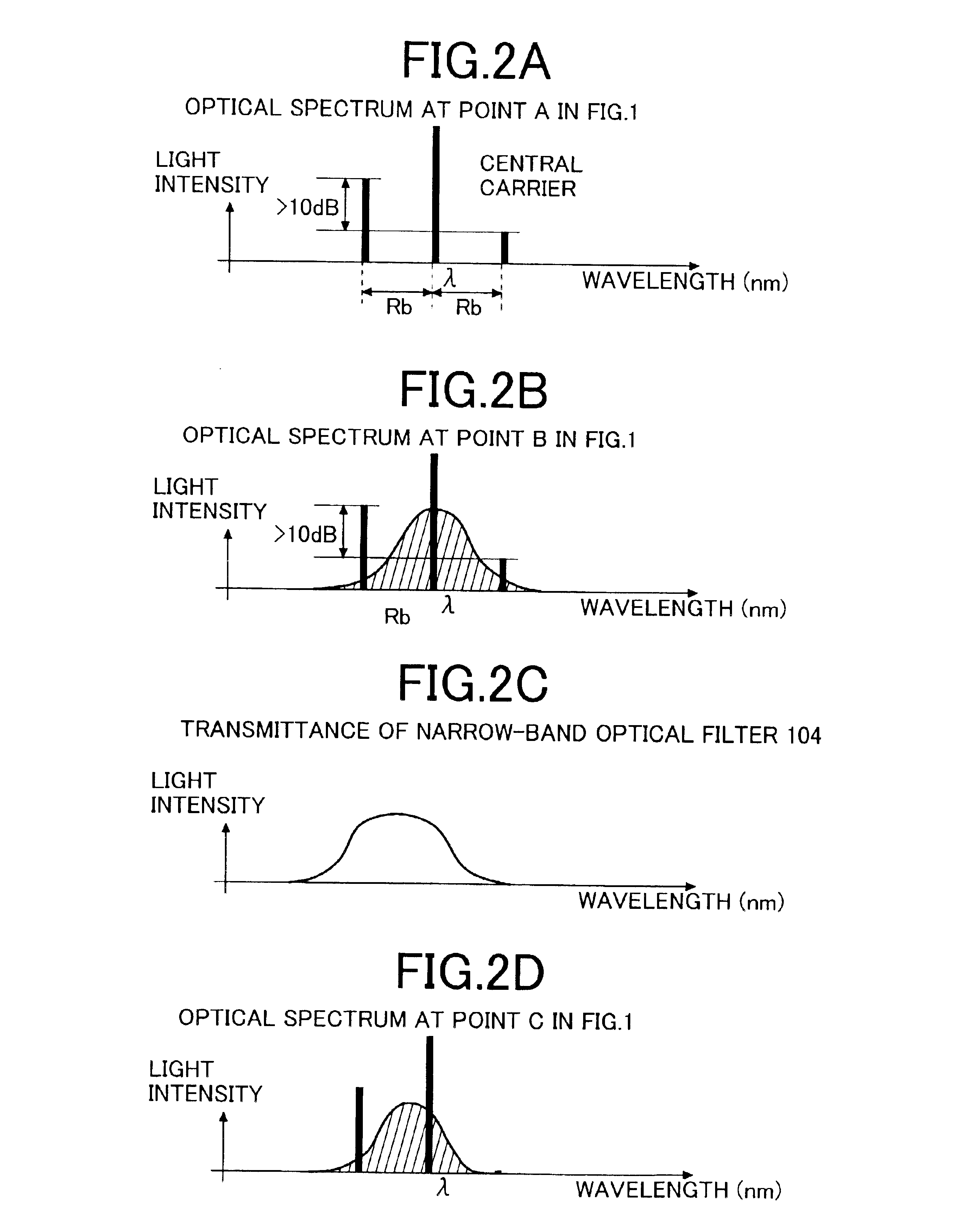
Further, the symmetry between the two drive signals can be easily maintained without allowing it to be destroyed, because the present invention merely has to maintain the symmetry of narrow-band sine wave signals. Furthermore, sideband suppression ratio reduction can be prevented by the present invention as it provides SSB modulation for a clock component and uses a narrow-band optical filter for the extraction of a signal's one sideband (VSB method).
As regards the problems with the conventional VSB optical transmitter, the present invention can prevent the narrow-band optical filter from suffering a significant loss, the received signal amplitude from decreasing, and the receiving sensitivity from degradation by subjecting only the signal of a clock component to single sideband modulation, for the purpose of reducing the amount of the component to be removed by the narrow-band optical filter.
The present invention also solves the waveform deterioration and receiving sensitivity degradation problems that are attributable to the optical filter shape and bandwidth error. The reason why this is possible is that the degree of waveform deterioration is minimized when a limited amount of carrier component is removed by the narrow-band optical filter, because the RZ signal waveform is mainly determined by a clock component.
As regards high-accuracy (about one-tenth of a signal bit rate; several gigahertz) wavelength stabilization for the difference between the optical signal wavelength and narrow-band filter transmission band center wavelength, the present invention does not encounter any problem even when the accuracy of wavelength stabilization more or less lowers because the carrier component, which most seriously affects the sideband suppression ratio and waveform, is suppressed beforehand. As to the necessity for complicated control for stabilizing the optical filter at a position that is offset from the signal center, the present invention can also exercise maximum value control to maximize the optical signal's filtered intensity because the optical signal is allowed to pass the optical filter with the carrier component suppressed beforehand to shift the center of gravity.

Problems solved by technology

Although the use of an L-band optical amplifier or Raman amplifier can increase the wavelength bandwidth several times, it lowers the pumping efficiency, which results, for instance, in a cost increase and a deterioration in the optical amplifier performance.
Although this method is widely used for radio communication, it has not been commercialized for optical fiber communication, and basic investigations concerning this method are currently conducted, for example, mainly by scientific societies.
However, RZ modulation generally requires a greater signal bandwidth than NRZ modulation, and it cannot increase the frequency density with ease.
In that sense, RZ modulation is disadvantageous in terms of spectral efficiency.
However, since this method entails high-frequency signal processing, significant waveform deterioration occurs.
As a result, the symmetry between the two drive signals 106-1, 106-2 is destroyed so that perfect sideband suppression is difficult to achieve.
This is the reason why this method cannot be readily implemented.
Further, this method is at a disadvantage in that it requires a complicated modulation circuit, which raises the cost of the transmitter.
Particularly, the RZ signal has about two times the electrical signal bandwidth of the NRZ signal and, therefore, entails higher-frequency signal processing, making expensive high-frequency component parts necessary.
At present, however, it is extremely difficult to fabricate a circuit that performs a Hilbert transform over the entire frequency range.
In this instance, however, the signal's low-frequency component is lost.
Consequently, digital signals used for normal optical fiber communication cannot be subjected to SSB conversion, which is a major problem for practical use.
In addition, the received signal amplitude lowers, thereby to degrade the receiving sensitivity due to the loss of the central carrier.
Therefore, if there is an error in the optical filter shape or bandwidth, waveform deterioration results, thereby reducing the receiving sensitivity.
It is extremely difficult to control these factors on the order of several gigahertz (approximately one-tenth of a signal bit rate).
If both of these wavelengths are in error, receiving sensitivity deterioration, crosstalk between neighboring wavelengths, or other significant performance deterioration results.
Particularly, the wavelength stabilization of an optical signal to a position spaced away from the optical filter center is susceptible to disturbances, such as intensity variations in an input optical signal or transmission characteristics changes with time.
Therefore, a control error is likely to occur.

Method used


Image

  • Optical single sideband transmitter
  • Optical single sideband transmitter
  • Optical single sideband transmitter

Examples


Embodiment Construction

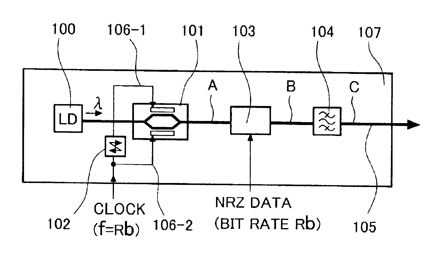
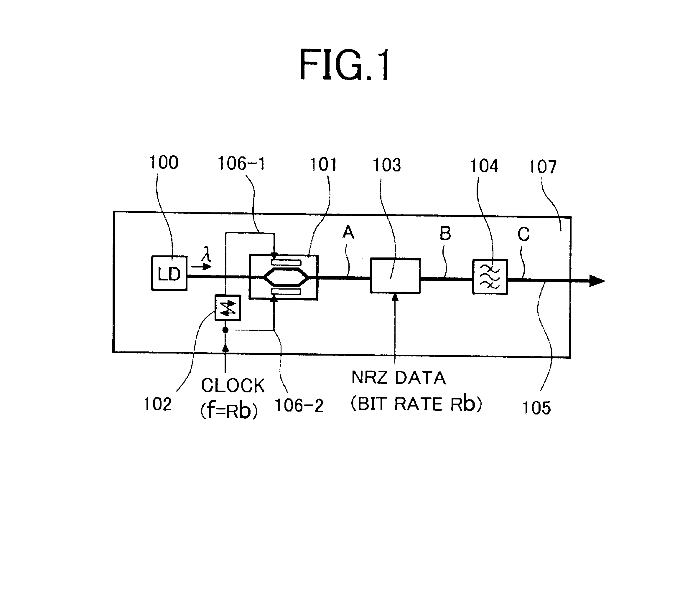
FIG. 1 is a schematic diagram that shows a first preferred embodiment of the present invention. It illustrates the structure of an optical single sideband transmitter in accordance with the present invention. When the structure of the first preferred embodiment is used, the light output (wavelength: λ) from a laser source 100 is applied to a dual-arm drive Mach-Zehnder optical modulator 101, and the light output thereof is supplied to an NRZ optical modulator 103. A sine wave clock signal (frequency: Rb and equal to the bit rate) within an electrical region is branched into two drive signals 106-1, 106-2 and applied to the two electrodes of the dual-arm drive Mach-Zehnder optical modulator 101. A DC bias component is applied to these two drive signals so as to produce an intensity modulation with their resulting amplitudes equalized. Further, these drive signals are rendered 90 degrees out of phase from each other by a phase shifter 102 (delay line). As a result, the laser light is ...


PUM


Abstract

With the normal modulation method, it is difficult to construct a Hilbert transform device because it is complicated. To solve the problem, a single sideband modulated optical pulse train is generated by driving a Mach-Zehnder optical modulator for optical pulse generation with a laser source's sine wave clock signals that have been rendered 90 degrees out of phase from each other. The generated pulse train is applied to an optical modulator, modulated with an NRZ (nonreturn-to-zero) data signal, and filtered by a narrow-band optical filter to obtain one of two sidebands.

Description

BACKGROUND OF THE INVENTIONThe present invention relates to an optical single sideband transmitter; and, more particularly, the invention relates to an optical single sideband modulation (SSB) method, which is used for bandwidth reduction of an RZ (return-to-zero) modulated optical signal as provided in optical information communication based on use of an optical fiber, and to the structure of an optical transmitter based on that method.The wavelength-division multiplexing (WDM) method, which provides optical information transmission by multiplexing a plurality of optical signals having to different wavelengths within an optical fiber, is an extremely effective means for increasing the capacity of optical fiber communication.In recent years, WDM (wavelength-division multiplexing) optical transmission equipment, having more than 100 wavelengths and a total transmission rate of higher than 1 Tbps, has been commercialized. Further, a transmission system having a tenfold number of wavel...

Claims


Application Information

Patent Timeline
IPC IPC(8): H04B10/155H04B10/152G02F1/025H04B10/516H04B10/54H04B10/61
CPCH04B10/505H04B10/5051H04B10/5053H04B10/506H04B10/508H04B10/50572H04L7/0008H04B2210/258
Inventor KIKUCHI, NOBUHIKOTAKEYARI, RYOJISUGAWARA, TOSHIKI
Owner HITACHI LTD
Learn More