Schottky diode static random access memory (DSRAM) device, a method for making same, and CFET based DTL

a static random access memory and diode technology, applied in semiconductor devices, digital storage, instruments, etc., can solve the problems of resistors consuming dc current, slow and unreliable holding information, and suffer from leakage, etc., to achieve stable load curve, less area, and faster than cfet design

Inactive Publication Date: 2005-02-08
SCHOTTKY LSI
View PDF5 Cites 23 Cited by
  • Summary
  • Abstract
  • Description
  • Claims
  • Application Information

AI Technical Summary

Benefits of technology

A more efficient circuit means has been proposed as viable approach to implement control logics with Diode Transistor Logic. Previously in the 1980s, DTL was once the backbone technology in Bipolar transistors. This invention teaches concepts to realize control functions and levels by various CFET and SBD configurations in additional to Buffer cell applications. Therefore is cost-performance attractive as a generic logic and memory tool-box suitable for any SOC applications. This design approach, using pulsed diode decoding and CFET inverter for NAND gates, takes less area, more stable load curve, and faster than CFET designs.

Problems solved by technology

The problem with this type of system is that it was slow and unreliable to hold information. FIG. 2 is a second-generation buffer storage system 30.
The resistor consumes DC current, and is slow when a large array capacity is involved.
But like its predecessors, it is also slow, and suffers from leakage. FIG. 4 is the latest generation of conventional buffer storage systems 70.
The problems with this type of system are large cell area, and it is difficult to scale down in operating voltage because of fixed high VT in the CFET.
The capacitances associated with every main circuit element intra and / or inter cell wise play an important role in speed considerations, and the noise margins are often compromised by the designers with speed in conjunction with the dc / ac power consumptions in the determination of Vcc supply, and signal and acceptable noise levels.

Method used


Image

  • Schottky diode static random access memory (DSRAM) device, a method for making same, and CFET based DTL
  • Schottky diode static random access memory (DSRAM) device, a method for making same, and CFET based DTL
  • Schottky diode static random access memory (DSRAM) device, a method for making same, and CFET based DTL

Examples


Embodiment Construction

The present invention relates generally to memory devices and in particular to the circuit design, device design, and processing technology of the high speed, high density, and low power physical constructs for memory cores, IO data buffer arrays, and control blocks.

The following description is presented to enable one of ordinary skill in the art to make and use the invention and is provided in the context of a patent application and its requirements. Various modifications to the preferred embodiment and the generic principles and features described herein will be readily apparent to those skilled in the art. Thus, the present invention is not intended to be limited to the embodiment shown but is to be accorded the widest scope consistent with the principles and features described herein.

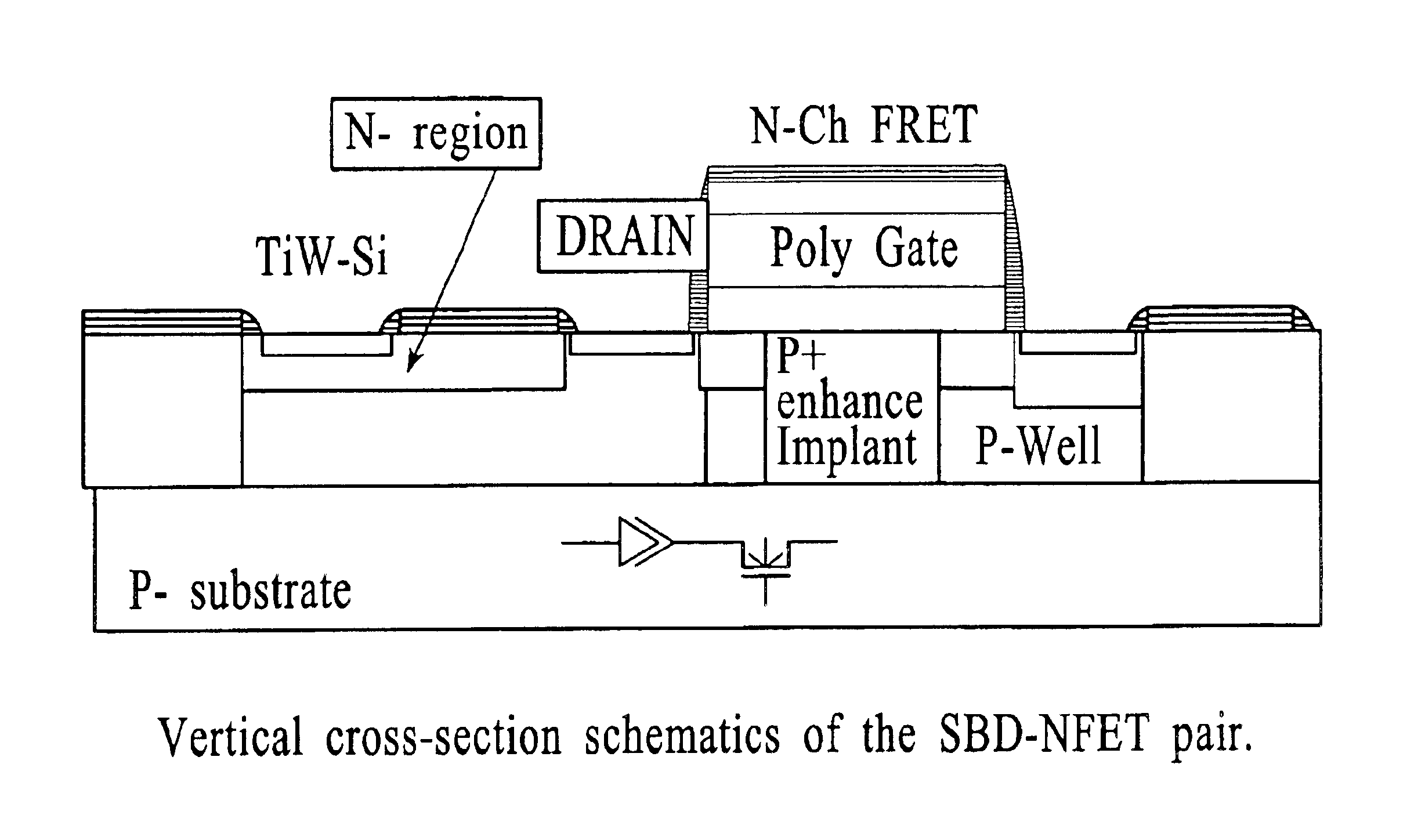
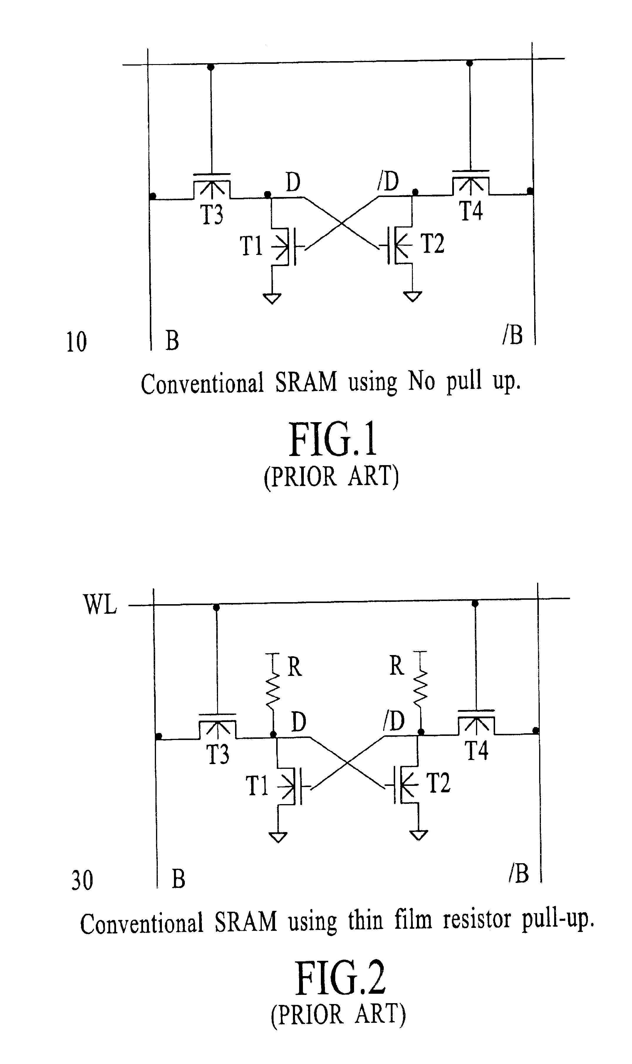
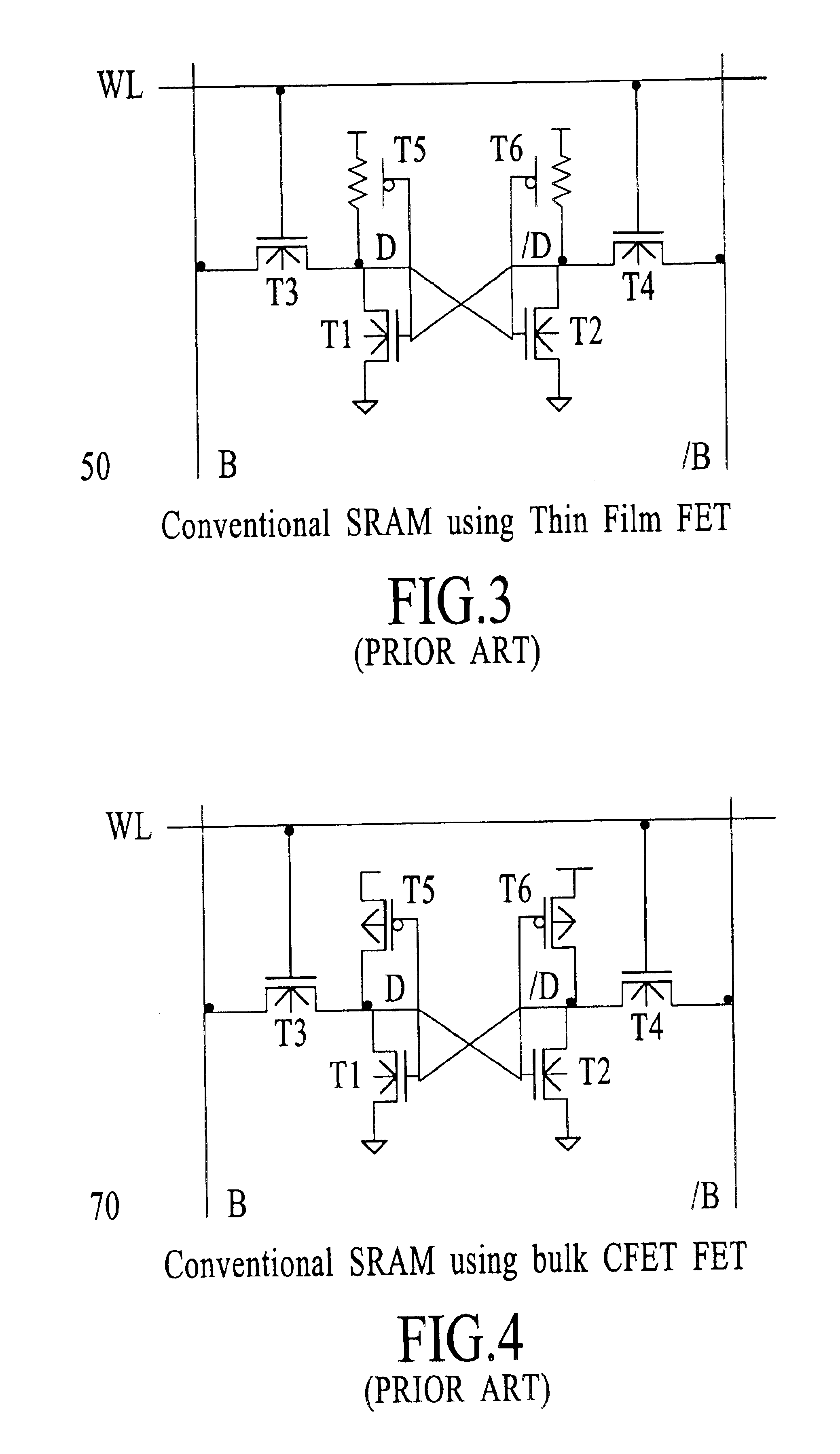
A high speed Static Random Access Memory Array which includes a 4-T cell and two Schottky Barrier Diodes (SBD) is disclosed (FIGS.5 and 6). In a preferred embodiment, the cell bulk area / speed advant...


PUM


Abstract

A high speed, low power Static Random Access Memory (SRAM) Array, which includes a 4T cell with two integrated Schottky Barrier Diodes (SBD) is provided. In a preferred embodiment, the cell bulk area and speed advantage is 30%, and AC power saving is 75% compared with the 6T CFET cell. The physical construct of the 4T cell saves capacitance in all critical nodes intra or inter cell wise, eliminates pass transistors, reduces the well noises. Typical embodiment uses a 0.15-um-rule based layout, and 1.5V supports operation at 5 ns cycles. SBD are used extensively with CFET to form a CMOS version of the Diode Transistor Logic circuitry. Generic control functions can be implemented including NAND/NOR gates, level shifting, decoding, voltage generator, ESD and latch-up protection, leakage control, and dynamic VT setting while in operation. Product applications include DRAM, SRAM, PLD, DRAM, CAM, Flash, Computing, Networking, and Communication devices as standalone system component or embedded into any ASIC.

Description

FIELD OF THE INVENTIONThe present invention relates generally to memory devices and in particular to the circuit design, device design, and processing technology of the high speed, high density, and low power physical constructs for memory cores, IO data buffer arrays, and control blocks.BACKGROUND OF THE INVENTIONConventional high speed and low power buffer storage systems have evolved over time. FIG. 1 illustrates a first generation buffer storage system 10. There are 2 NFET pass transistors and 2 CFET, which formed a latch. The system 10 uses no pull-up transistors for the latch portion of the cell. The problem with this type of system is that it was slow and unreliable to hold information. FIG. 2 is a second-generation buffer storage system 30. In this system 30 the SRAM cell using high value resistor pull up. The resistor consumes DC current, and is slow when a large array capacity is involved. As the density gets higher, it consumes large DC current and the circuit is slow. FI...

Claims


Application Information

Patent Timeline
Patent Type & Authority Patents(United States)
IPC IPC(8): G11C11/412
CPCG11C11/412
Inventor CHANG, AUGUSTINE WEI-CHUN
Owner SCHOTTKY LSI
Why Eureka
Try Eureka