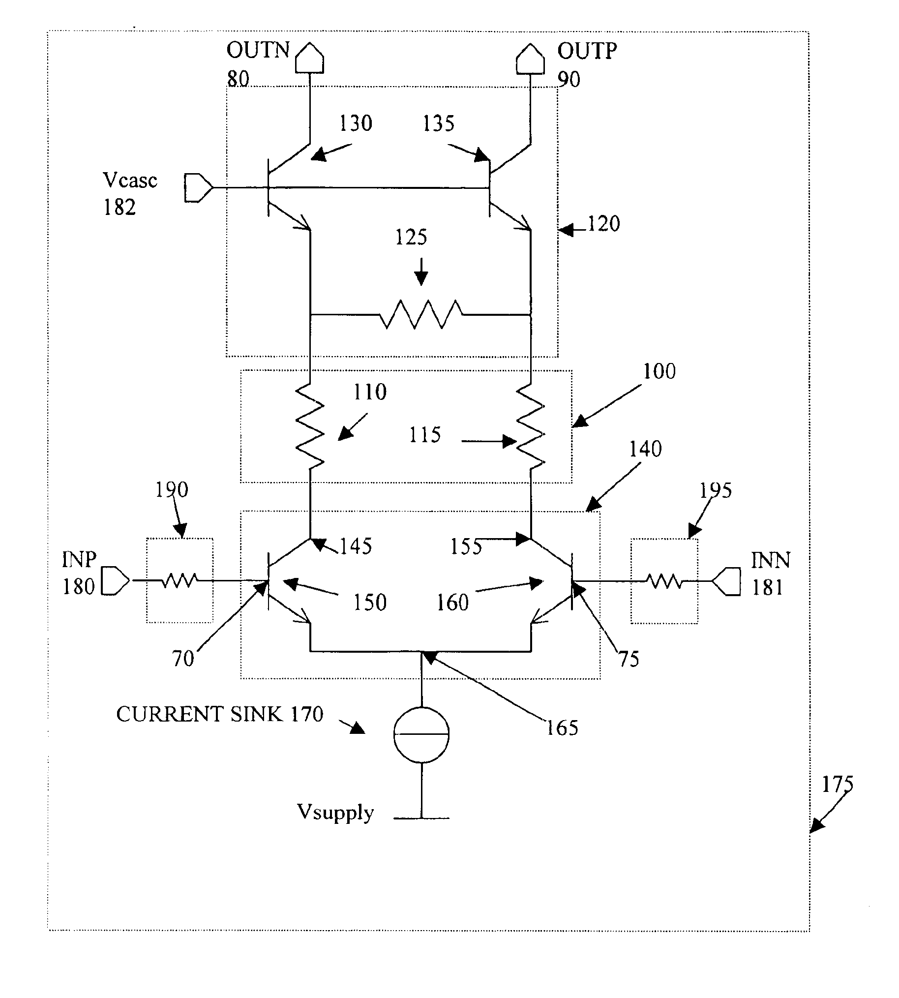
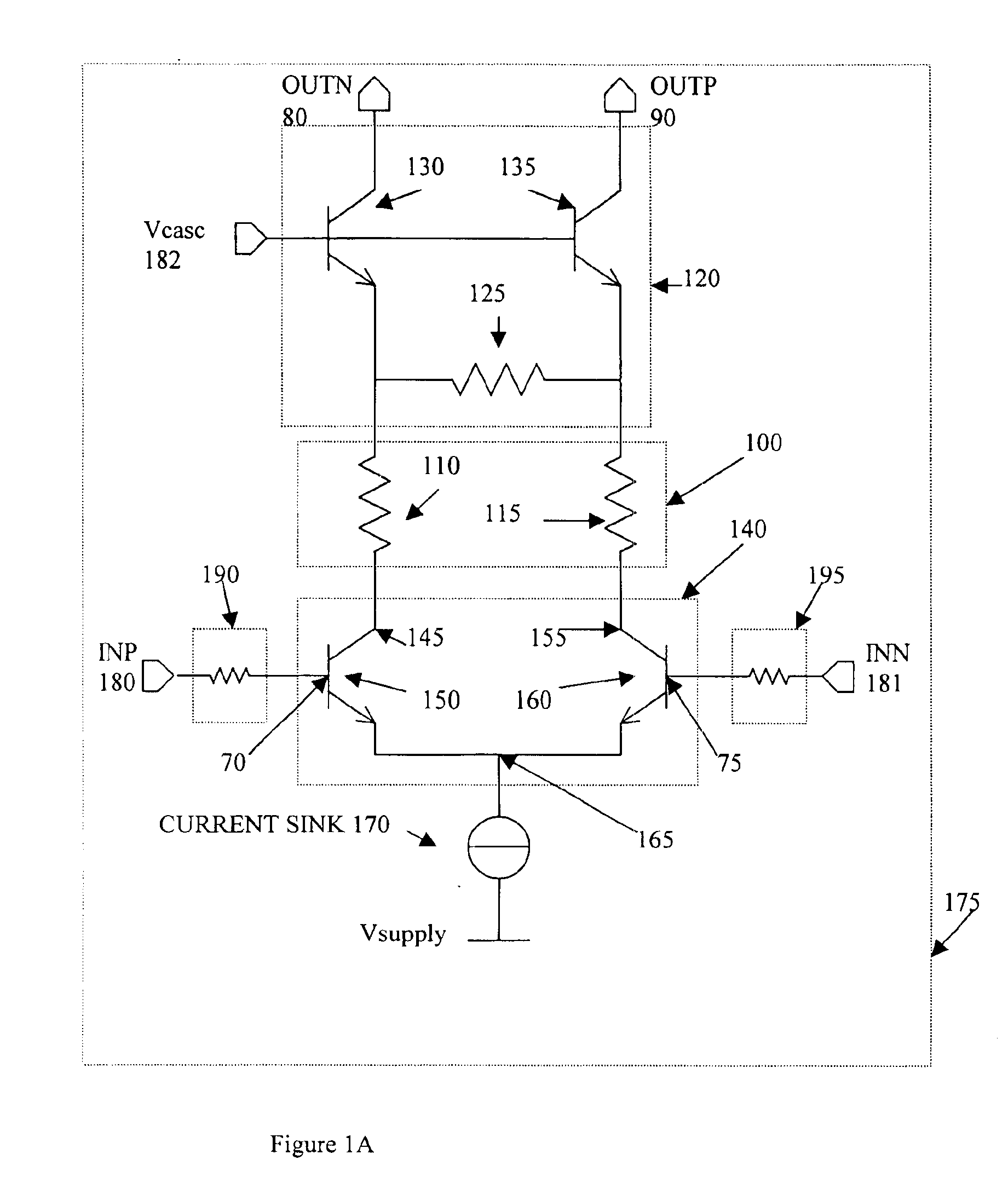
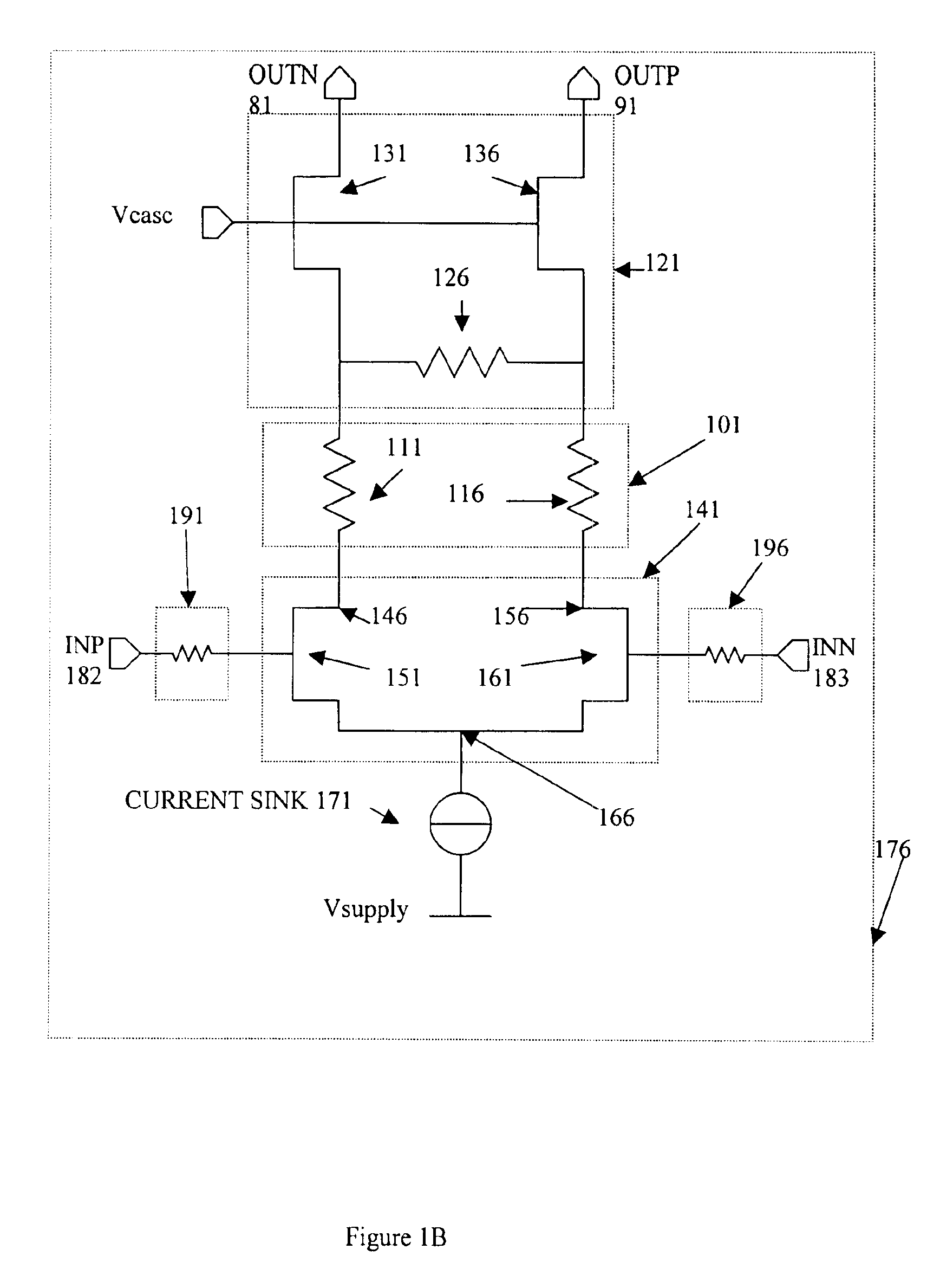
It is an object of the current invention to provide a robust differential output buffer component designed to operate over a wide frequency range, capable of providing two high quality output signals even when provided with variable and / or poor quality differential input signals.
According to the current invention, the buffer component comprises a cascode module for receiving a differential current signal from a differential pair module and transmitting that differential signal as two output currents. Preferably, these two output currents are converted to two output voltages by two external load impedances. Often, in addition, “back termination” impedances may be present on-
chip to minimize the
impact of signal reflections in case of imperfect external termination. Typically, the differential pair module external to the current invention and the cascode module internal to the current invention may comprise sets of bipolar transistors and / or sets of
field effect transistors (FETs). Using the example of a bipolar implementation, the emitter end of a
common base cascode pair is coupled to the collector end of a
common emitter differential pair. The resistance at the collector nodes of the differential pair is due in part to the characteristics of the cascode pair. Optionally, a resistive module, called a cascode resistive module, may be inserted between the cascode pair and the differential pair to further alter the resistance at the collector nodes of the differential pair. Additionally, the resistance due to the stage driving the differential pair may be engineered to alter the properties of the buffer output waveform. In some cases, optional resistive modules, called drive resistive modules, may be coupled to the inputs of the differential transistors (base nodes for bipolar implementations or gate nodes for FET implementations) to provide an additional small resistance for altering the properties of the buffer output waveform. According to the current invention, for each of the output signals of the high-speed buffer element, the symmetry of the rising waveform edge with respect to the falling waveform edge may be engineered. Continuing with the example of a bipolar implementation, the symmetry of the output signal waveforms may be manipulated by
engineering three parameters:1) the cascode bias2) the resistance at the collector nodes of the differential pair3) the resistance at the base nodes of the differential pair.
By
engineering these three parameters, the average base-collector
voltage, the
voltage swing of the collector nodes of the
transistor pair, and the symmetry of the input waveforms may be controlled, thereby providing substantial, self-controlled
capacitance changes at the differential pair's collector nodes. This technique may be used to suppress effects due to the undesirable
common mode signal component of the two output signals. For either of the buffer output voltages, this technique may be used to alter the symmetry of the rising and falling edges as represented by the Vcross,out in an eye diagram. Whereas typical buffer component designs may minimize the resistances at the input and output nodes of the differential pair to minimize delays, according to the current invention, the shape of the output signal waveforms may be engineered and / or improved by altering these resistances.
Preferably, the current invention may be used to improve the quality of the two output signals of a high-speed differential buffer component by improving the symmetry of the output signals under expected operating conditions. However, according to an alternate embodiment of the current invention, the output signals may be engineered to alter the symmetry in other ways. For example, according to the current invention, the output signals may be purposely pre-distorted to compensate for opposite distortions expected from an
electronic circuit driven by this buffer.
Optionally, preconditioning the input signals to the differential pair module with a Cherry-Hooper style
amplifier (for example, see E. M. Cherry and D. E. Hooper, “The Design of Wide-band
Transistor Feedback Amplifiers,” Proc. I.E.E., vol. 110, No. 2, February 1963, pp. 375-389) may further improve the quality of the output signals provided by the current invention. This may be especially true for poor quality input signals with a substantial and / or inconsistent amplitude variation and / or a common mode component.


