
Semiconducting oxide nanostructures

a technology of semiconducting oxide and nanostructure, which is applied in the field of nanostructures, can solve the problems of uncontrollable properties, difficult control of the structure and morphology of many nanostructures, and difficult investigation of wire-like semiconducting oxide nanostructures

Inactive Publication Date: 2005-03-08
GEORGIA TECH RES CORP
View PDF1 Cites 32 Cited by
  • Summary
  • Abstract
  • Description
  • Claims
  • Application Information

AI Technical Summary

Benefits of technology

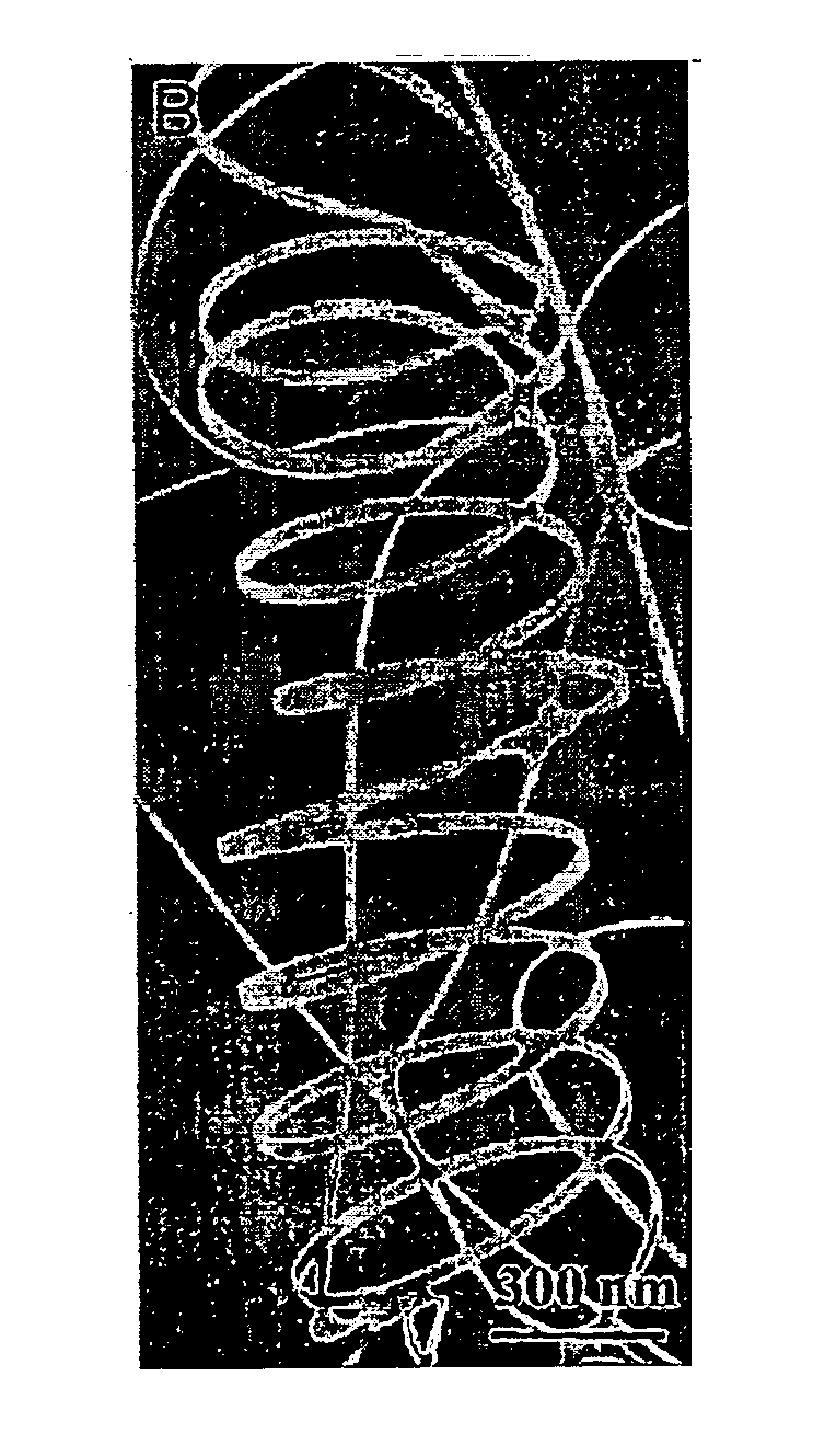
This patent describes new types of nanostructures and methods of making them. The nanostructures include a free-standing, helical semiconductor oxide nanostructure and a free-standing semiconductor oxide nanoring. The methods involve heating a metal oxide powder mixture and flowing an inert gas over it to form the nanostructures. These nanostructures have a substantially rectangular cross-section and can be used in various applications.

Problems solved by technology

In contrast, investigations of wire-like semiconducting oxide nanostructures can be difficult due to the unavailability of nanowire structures.
However, the nanostructures discussed above can have a variety of deficiencies.
For example, often it is difficult to control the structure and morphology of many nanostructures.
These deficiencies can cause problems such as, for example, uncontrolled properties due to uncontrolled structure and / or morphology, scattering from dislocations in electric transport applications, and degraded optical properties.
Thus, a heretofore unaddressed need exists in the industry to address at least the aforementioned deficiencies and / or inadequacies.

Method used


Image

  • Semiconducting oxide nanostructures
  • Semiconducting oxide nanostructures
  • Semiconducting oxide nanostructures

Examples


example 1a

Zinc Oxide

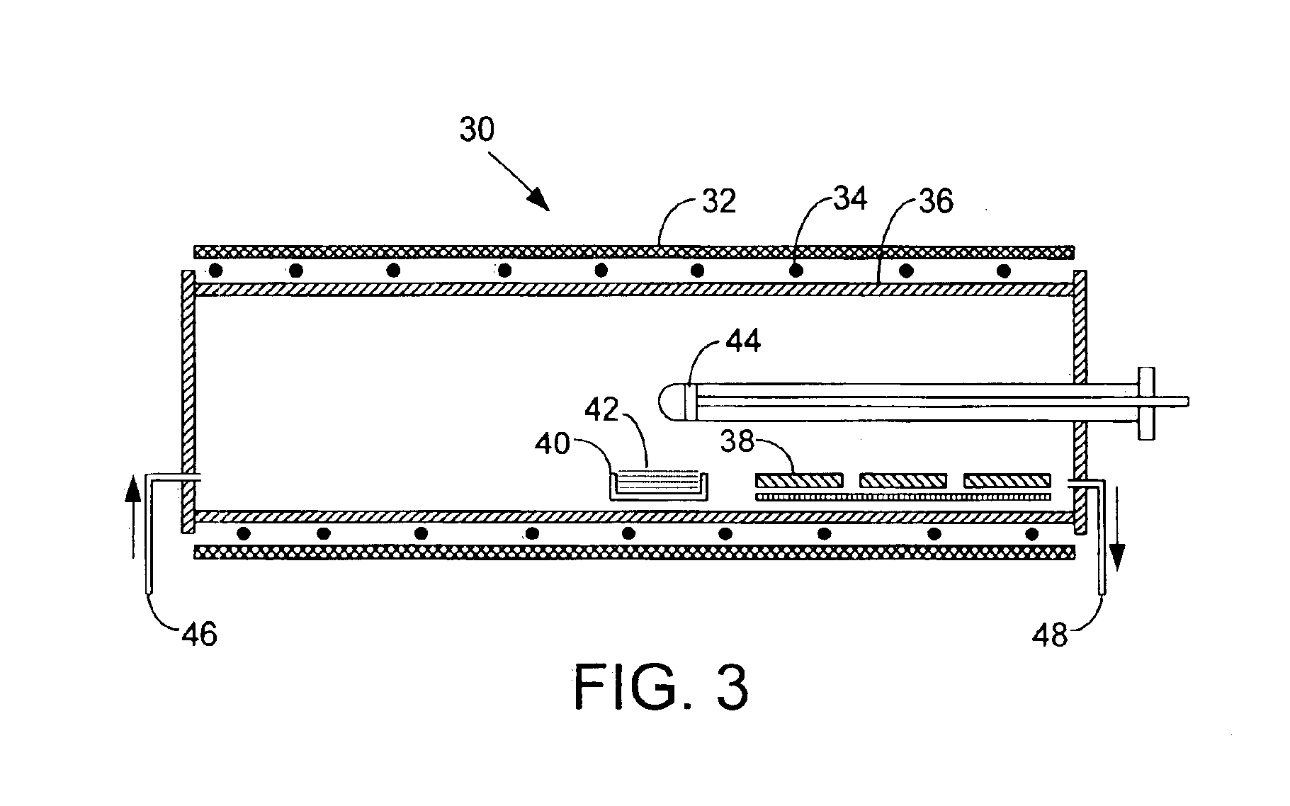
Thermal evaporation of zinc oxide (ZnO) powders (purity: 99.99%, melting point: 1975° C.) at 1400° C. for approximately 2 hours resulted in white wool-like products that formed in high yield on the surface of the alumina plate 38. Scanning electron microscopy (SEM) observations reveal that the products consist of a large quantity of nanostructures with typical lengths in the range of several tens to several hundreds of micrometers, while some of nanostructures have lengths on the order of millimeters. EDS microanalysis and powder XRD measurement show that the sample is wurtzite (hexagonal) structured ZnO with lattice constants of a=3.249 Å and c=5.206 Å, consistent with the standard values for bulk ZnO.

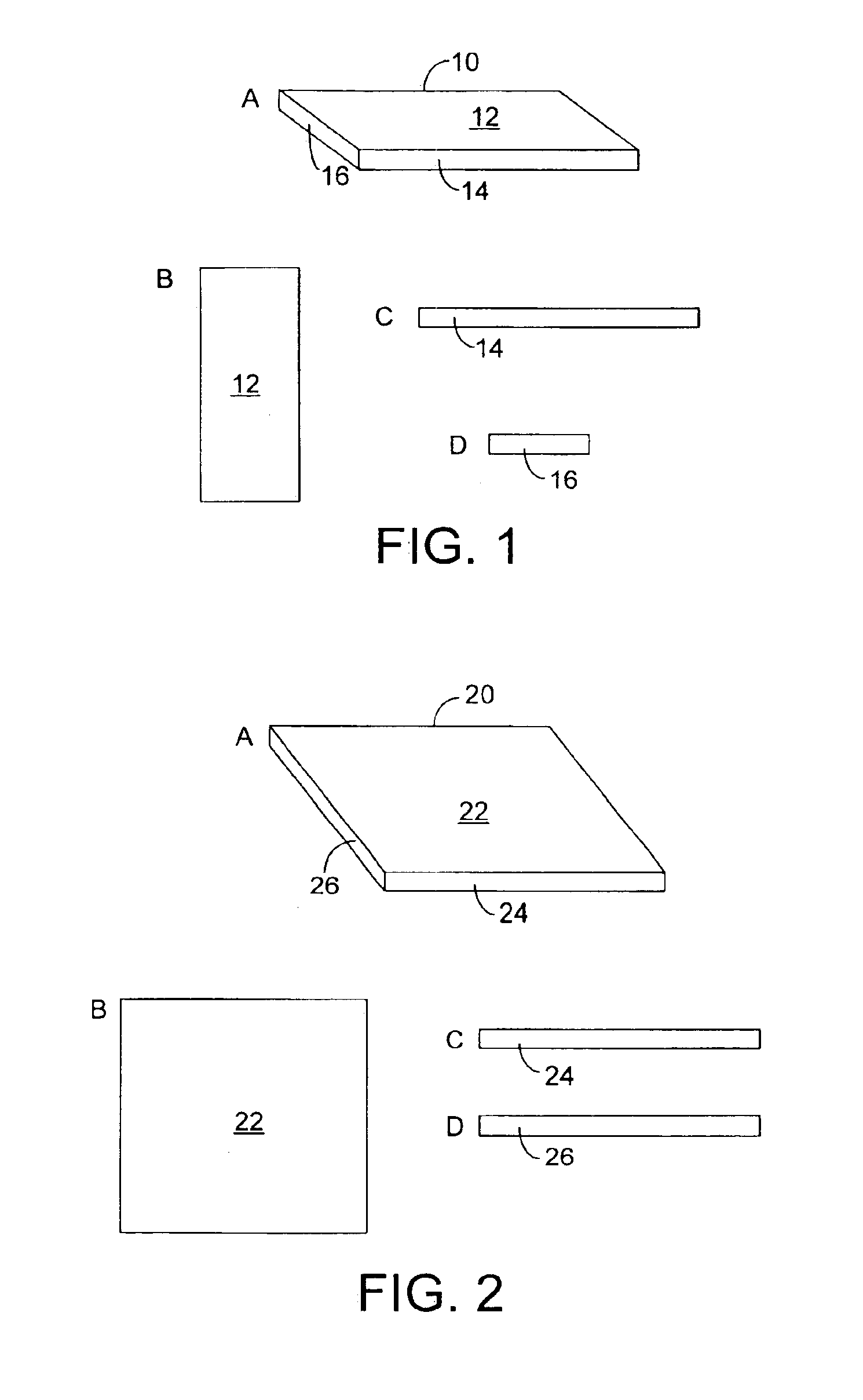
TEM images reveal that the ZnO nanostructure has a substantially rectangular cross-section (i.e., nanobelt) that is distinct in cross-section from nanotubes and nanowires. Each nanobelt has a uniform width along a substantial portion of the length of the nanobelt, and the ty...

example 1b

Zinc Oxide

Zinc oxide (ZnO) is a versatile “smart” material that has applications in catalysts, sensors, piezoelectric transducers, transparent conductor, and surface acoustic wave devices. The non-central symmetry and the tetrahedrally coordinated ZnO4 unit in ZnO result in anisotropic piezoelectric properties. Structurally, the wurtzite structured ZnO crystal is described schematically as a number of alternating planes composed of fourfold coordinated O2− and Zn2+ ions, stacked alternatively along the c-axis. The oppositely charged ions produce positively charged (0001)-Zn and negatively charged (000{overscore (1)})-O polar surfaces, resulting in a normal dipole moment and spontaneous polarization, as well as a divergence in surface energy. To maintain a stable structure, the polar surfaces generally have facets or exhibit massive surface reconstructions, but ZnO ±(0001) is an exception, which is atomically flat, stable, and without reconstruction.

Nanowire and nanotube based materi...

example 1c

Zinc Oxide

Self-assembly is a fundamental approach for organizing and constructing hierarchical structures using nano-building-blocks through substrate patterning and surface functionalization. Self-assembly of nanocrystals is driven by van der Walls forces and hydrogen bonding among the passivating organic molecules on the particle surfaces. Polar-charge induced self-assembly is frequently observed for chain molecules in a solution environment: a local spontaneous ordering of molecular polarity and chirality resulting in the formation of stripes; and chiral domains of achiral molecules and ferroelectric liquid crystals being polarization-induced self-assembly. For crystalline nanomaterials grown in a solid-vapor environment, one type of polar-charge induced helical and spiral structures of ZnO has been done (see Example 1B). In this example, a distinct and unique nanoring structure that is formed by spontaneous self-coiling of a polar nanobelt during growth is described. Although no...


PUM

PropertyMeasurementUnit
heightaaaaaaaaaa
widthaaaaaaaaaa
widthaaaaaaaaaa

Abstract

Briefly described, new types of nanostructures and methods of fabrication thereof are disclosed. A representative nanostructure includes a free-standing, helical semiconductor oxide nanostructure. The free-standing, helical semiconductor oxide nanostructure includes a nanobelt having a substantially rectangular cross-section. The the nanobelt is about 5 nanometers to about 200 nanometers in width and about 3 nanometers to about 50 nanometers in height, and the radius of the helical semiconductor oxide nanostructure is about 200 to 5000 nanometers.

Description

TECHNICAL FIELDThis disclosure is generally related to nanostructures and, more particularly, is related to semiconductive and piezoelectric oxide nanostructures and fabrication thereof.BACKGROUNDBinary semiconducting oxides often have distinctive properties and can be used as transparent conducting oxide (TCO) materials and gas sensors. Current studies of semiconducting oxides have been focused on two-dimensional films and zero-dimensional nanoparticles. For example, fluorine-doped tin oxide films are used in architectural glass applications because of their low emissivity for thermal infrared heat. Tin-doped indium oxide (ITO) films can be used for flat panel displays (FPDs) due to their high electrical conductivity and high optical transparency; and zinc oxide can be used as an alternative material for ITO because of its lower cost and easier etchability. Tin oxide nanoparticles can be used as sensor materials for detecting leakage of several inflammable gases owing to their high...

Claims


Application Information

Patent Timeline
Patent Type & Authority Patents(United States)
IPC IPC(8): C01G21/00C01G11/00C01B13/14C01G21/02C01G19/00C01G15/00C01G19/02H02K31/00H02K31/02C30B29/64
CPCB82Y30/00C01G11/00C01G15/00C01G19/02C01G21/02H02K31/02C01B13/145Y10T428/265C01P2002/76C01P2002/77C01P2004/10C01P2004/20C01P2004/22C01P2004/54C01P2004/62C01P2004/64Y10S977/765Y10T428/2973Y10T428/24
Inventor WANG, ZHONG LINKONG, XIANGYANG
Owner GEORGIA TECH RES CORP
Learn More