Method of forming a fuse

a technology of fuse and insulating pad, which is applied in the direction of semiconductor devices, semiconductor/solid-state device details, electrical apparatus, etc., can solve the problems of poor step coverage ability, limiting factor of traditional al/sio/sub>interconnect system, and insatiable, so as to reduce the thickness of the fuse and improve the uniformity of the thickness , the effect of bondability of the bonding pad during the packaging process

Inactive Publication Date: 2005-03-08
MARLIN SEMICON LTD
View PDF4 Cites 18 Cited by
  • Summary
  • Abstract
  • Description
  • Claims
  • Application Information

AI Technical Summary

Benefits of technology

It is an advantage of the claimed invention that the method of forming the fuse is to form a fuse opening by removing the third dielectric layer on top of the fuse with a fuse mask and an additional photo-etching-process. Then an anisotropic dry etching process is performed to remove a predetermined thickness of the metal layer underneath the fuse opening. After that an oxide layer is formed on the surface of the semiconductor substrate. Finally a passivation opening is formed by utilizing a pad mask and another photo-etching-process. As a result, the thickness for the fuse is reduced, due to the additional photo-etching-process and the subsequent anisotropic dry etching process, without adding any metal deposition process. Hence the aluminum layer will not be too thick to sever. In addition, the oxide layer on top of the fuse is formed by a deposition process, and its thickness uniformity is better than the oxide layer formed by the traditional etching back process. Moreover, the bondability of the bonding pad during packaging process is maintained because the thickness for the aluminum bonding pad remains at the thickness for the original metal layer. These and other objectives of the present invention will no doubt become obvious to those of ordinary skill in the art after reading the following detailed description of the preferred embodiment, which is illustrated in the various figures and drawings.

Problems solved by technology

However, as ICs have relentlessly marched down the path towards smaller geometry and to a deep sub-micron generation in the pursuit of increased speed, the traditional Al / SiO2 interconnect system has shown itself to be a limiting factor.
The reason is that aluminum is usually formed by a DC magnetron sputtering process, which is characterized by its poor step coverage ability.
In the process generation beyond 0.13 μm, line width is smaller, aspect ratio is relatively increased, and the poor step coverage ability causes a severe problem.
Although a high temperature (>400° C.) aluminum process with an improved step coverage ability due to a high surface migration rate at high temperature has been developed, it is not satisfactory.
However, aluminum is easily deposited and etched, and is very cheap as well.
Although the metal lines composed of copper are superior to the metals composed of aluminum in terms of electrical performance, the etching process for copper cannot be done in a chemical way because of the poor volatile ability of copper-chloride-alloy, which is a drawback of copper metal lines.
However, copper is difficult to evaporate during the laser zip process because of its high melting point.
A splash phenomenon results and causes difficulty in assuring high reliability.
To increase the thickness of aluminum brings difficulty to the process, and it is difficult to sever the fuse.
However, the higher the energy of laser beam, the higher probability of damaging the structure underneath.
If the composition material in the via hole is aluminum, its poor step coverage ability easily induces problems.

Method used


Image

  • Method of forming a fuse
  • Method of forming a fuse
  • Method of forming a fuse

Examples


Embodiment Construction

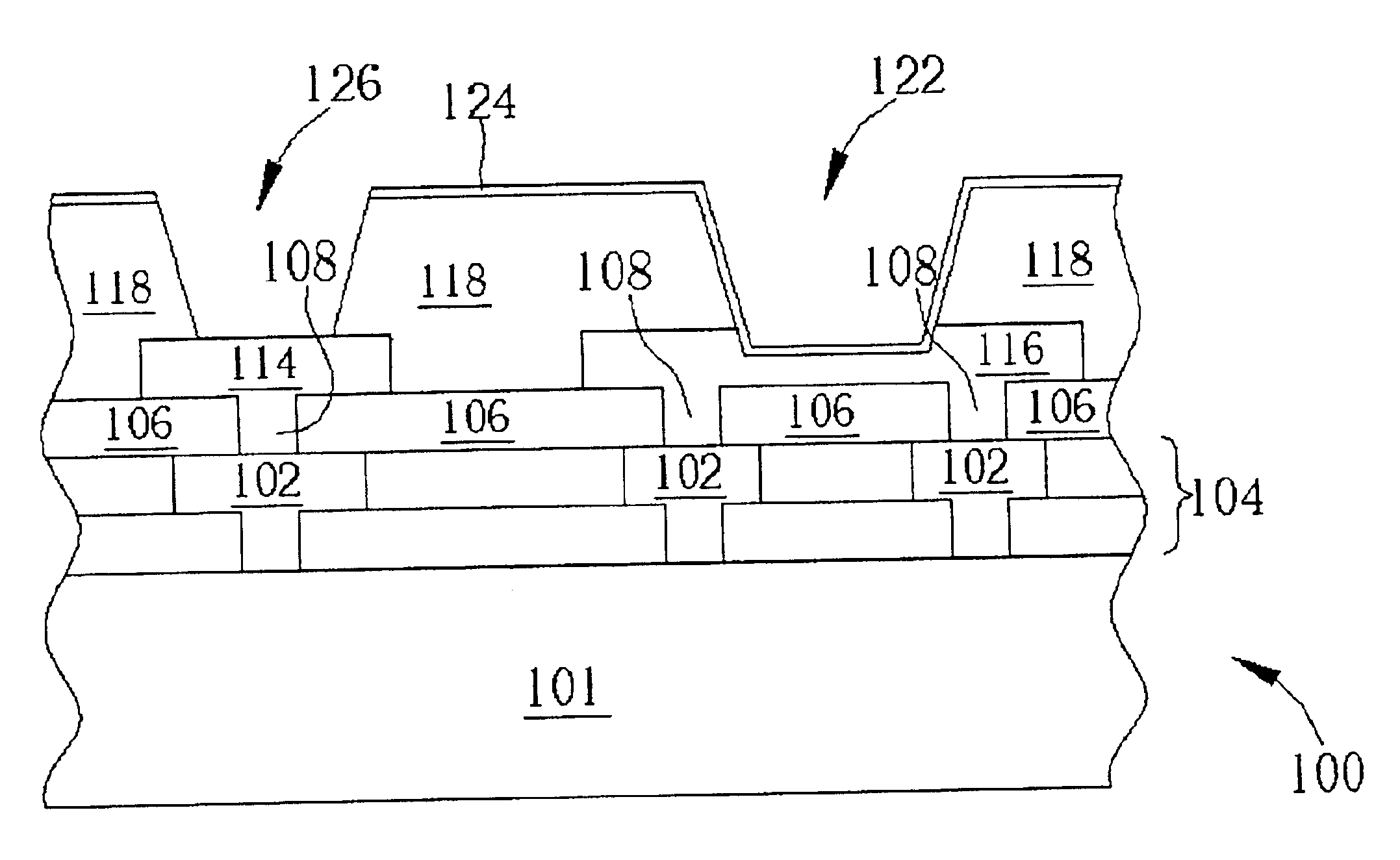
Please refer to FIG. 5 through FIG. 9. FIG. 5 through FIG. 9 are schematic diagrams showing the formation of a fuse 116 on a semiconductor wafer 100 according to the present invention method. As shown in FIG. 5, the semiconductor wafer 100 comprises a silicon substrate 101. At least one memory cell (not shown) or at least one transistor (not shown) is formed on the silicon substrate 101. The present invention method is to form individual metal lines 102 on the silicon substrate 101 first. Different metal lines 102 are isolated by a first dielectric layer 104. The metal line 102 comprises a metal interconnection electrically connected to a conductive plug or a dual damascence structure conductor. The metal lines 102 are composed of aluminum or copper. In the case where aluminum is used, a continuous process including deposition, photolithography, and etching is utilized. In the case where copper is used, a dual damascence process is usually used.

As mentioned previously, aluminum is u...


PUM


Abstract

A surface of a semiconductor substrate defined with at least one fuse area and at least one bonding pad area. A conductive layer with a thickness of 12 kÅ and a protective layer are sequentially formed on the surface of the semiconductor substrate. Then portions of the protective layer and portions of the conductive layer in the fuse area are etched to make the thickness for the remaining conductive layer in the fuse area be approximately 5 kÅ. Finally a dielectric layer is formed on the surface of the semiconductor substrate, and portions of the first dielectric layer and portions of the protective layer in the bonding pad area are etched until reaching the top surface of the conductive layer.

Description

BACKGROUND OF INVENTION1. Field of the InventionThe present invention relates to a method of forming a fuse, and more particularly, to a method of forming fuse and bonding pad with a single-layered aluminum metal and two photo-etching-processes (PEP).2. Description of the Prior ArtAluminum alloys with silicon dioxide (SiO2) dielectrics have been the materials of choice for interconnect systems since the dawn of the integrated circuit (IC) era. These materials were convenient to process using mature subtractive etch processes for metal line patterning. However, as ICs have relentlessly marched down the path towards smaller geometry and to a deep sub-micron generation in the pursuit of increased speed, the traditional Al / SiO2 interconnect system has shown itself to be a limiting factor. Cu-dual damascene architectures with low-k dielectrics are thus developing and becoming the norm now in forming interconnects. Overall, RC delays occurring during signal transmission are reduced and op...

Claims


Application Information

Patent Timeline
Patent Type & Authority Patents(United States)
IPC IPC(8): H01L23/525H01L23/52H01L21/02H01L21/60
CPCH01L23/5258H01L2924/0002H01L2924/00
Inventor LEE, CHIU-TEWU, TE-YUAN
Owner MARLIN SEMICON LTD
Why Eureka
Try Eureka