Large size semiconductor crystal with low dislocation density

a technology of dislocation density and large semiconductor crystal, which is applied in the direction of crystal growth process polycrystalline material growth, etc., can solve the problems of large compound semiconductor crystal production, large furnace size, and inability to produce large compound semiconductor crystal greater than 4 inches, so as to reduce the activation factor and reduce the residual strain , the effect of improving the device performan

Inactive Publication Date: 2005-03-15
SUMITOMO ELECTRIC IND LTD
View PDF27 Cites 10 Cited by
  • Summary
  • Abstract
  • Description
  • Claims
  • Application Information

AI Technical Summary

Benefits of technology

The advantage of the present invention is most appreciable when a semiconductor single crystal is grown by the VB method. According to the present invention, a semiconductor crystal at least 6 inches in diameter with the average dislocation density of not more than 1×104 cm−2 can easily be obtained. By controlling the cooling method and the like, a semiconductor crystal having an average dislocation density of approximately 1 to 5×103 cm−2 can be grown. The electrical property can be made uniform by such a low dislocation density.
Furthermore, according to the present invention, a semiconductor crystal with the concentration of boron (B) less than 3×1016 cm−3, preferably not more than 1×1016 cm−3 can be grown. It is said that boron (B) reduces the activation factor after ion implantation. Therefore, the device performance can be improved by reducing the concentration of boron (B).
The semiconductor crystal of the present invention has a low residual strain since the occurrence of dislocation is low. Therefore, the strength sufficient for practical usage can be achieved with the thickness of 500-700 μm even when the size becomes greater. The average residual strain of the substrate measured using the photoelastic effect is not more than 1×10⁻⁵.
The semiconductor crystal of the present invention as an ingot is characterized in that the deviation of the carbon concentration in the direction of the length is extremely small. In other words, the carbon (C) concentration distribution can be made uniform along the direction of the length by controlling the concentration of the CO gas in the reactor tube. According to the present invention, a compound semiconductor single crystal ingot can be obtained that has a diameter of at least 6 inches, the average dislocation density of less than 1×104 cm−1, and having the carbon concentration restricted to be within ±50% with respect to the target value over the region of 0.1-0.8 in fraction solidified. In other words, when the carbon concentration is set to 1×1015 cm−3, for example, the carbon concentration of the actually obtained crystal has variation of the carbon concentration restricted within ±50% with respect to the set value over the entire length. Therefore, there is the advantage that the yield is improved when the substrate is cut out from this ingot. The reason why variation in the carbon concentration can be reduced by the present invention is due to the critical controllability of the concentration of the CO gas in the reactor tube during the growth. This advantage becomes more effective by selecting a material that does not include carbon for the reactor tube or by coating the reactor tube with a material that does not include carbon. Furthermore, a carbon heater is not used in the present invention in contrast to the case of crystal growth by the conventional high pressure chamber. This means that a crystal can be grown with the interior of the reactor tube under a carbon-free condition. Therefore, the distribution of the carbon concentration can be made uniform.
An example of producing a semiconductor crystal of 6 inches in diameter will be described hereinafter. However, the present invention is applicable to production of a semiconductor crystal of a larger size such as 8 inches.
The first embodiment is characterized in that the heater is not externally shielded, as shown in FIG. 1. According to the conventional LEC method as disclosed in the aforementioned Japanese Patent Laying-Open No. 2-233578, a carbon heater of low reactivity was used to grow a crystal within a high pressure chamber. In contrast, the first embodiment of the present invention has a heater provided in the atmosphere outside the reactor tube. Therefore, a heater based on iron and the like that is low in cost can be used. This type of heater can easily provide multi zones. Therefore, favorable controllability of a temperature distribution can be provided. When a carbon heater is not used, a crystal can be grown with the interior of the silicon carbide reactor tube under a carbon-free state. Therefore, variation in the carbon concentration in the crystal can be reduced.

Problems solved by technology

However, there are many problems on the mass production of a large compound semiconductor crystal.
Production of a large compound semiconductor crystal greater than 4 inches is not yet practical.
Accordingly, the size of the furnace becomes larger to increase the furnace cost.
Thus, there is a problem that the furnace cost is increased.
In the case where the quartz ampoule shown in FIG. 16 is used, there was a problem that it is difficult to produce a large crystal by charging a great amount of the material since there is a possibility of deformation or breakage of the ampoule.
There is also a problem that the material cannot be synthesized, in situ, since the ampoule is sealed, barring the application of the As injection method.
There is also the problem that the atmospheric gas cannot be controlled after the ampoule is sealed.
However, the heat-proof sealing member has poor airtightness, so that sufficient difference between the inside pressure and the outside pressure cannot be achieved.
However, this publication is completely silent about using silicon carbide for the reactor tube.

Method used


Image

  • Large size semiconductor crystal with low dislocation density
  • Large size semiconductor crystal with low dislocation density
  • Large size semiconductor crystal with low dislocation density

Examples


first embodiment

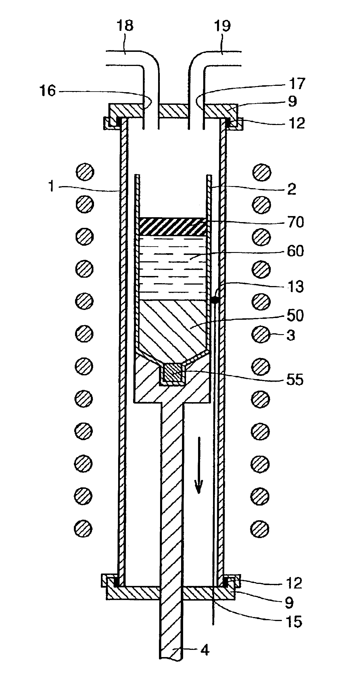
FIG. 1 is a sectional view of the schematic structure of an apparatus of producing a semiconductor crystal according to a first embodiment of the present invention.

Referring to FIG. 1, the apparatus includes a silicon carbide reactor tube 1 and a kanthal heater 3. Silicon carbide reactor tube 1 has an inner diameter of 170 mm and a thickness of 3 mm with an open end at both end sides. Kanthal heater 3 is arranged around reactor tube 1 in the atmosphere with 5 zones.

The first embodiment is characterized in that the heater is not externally shielded, as shown in FIG. 1. According to the conventional LEC method as disclosed in the aforementioned Japanese Patent Laying-Open No. 2-233578, a carbon heater of low reactivity was used to grow a crystal within a high pressure chamber. In contrast, the first embodiment of the present invention has a heater provided in the atmosphere outside the reactor tube. Therefore, a heater based on iron and the like that is low in cost can be used. This t...

second embodiment

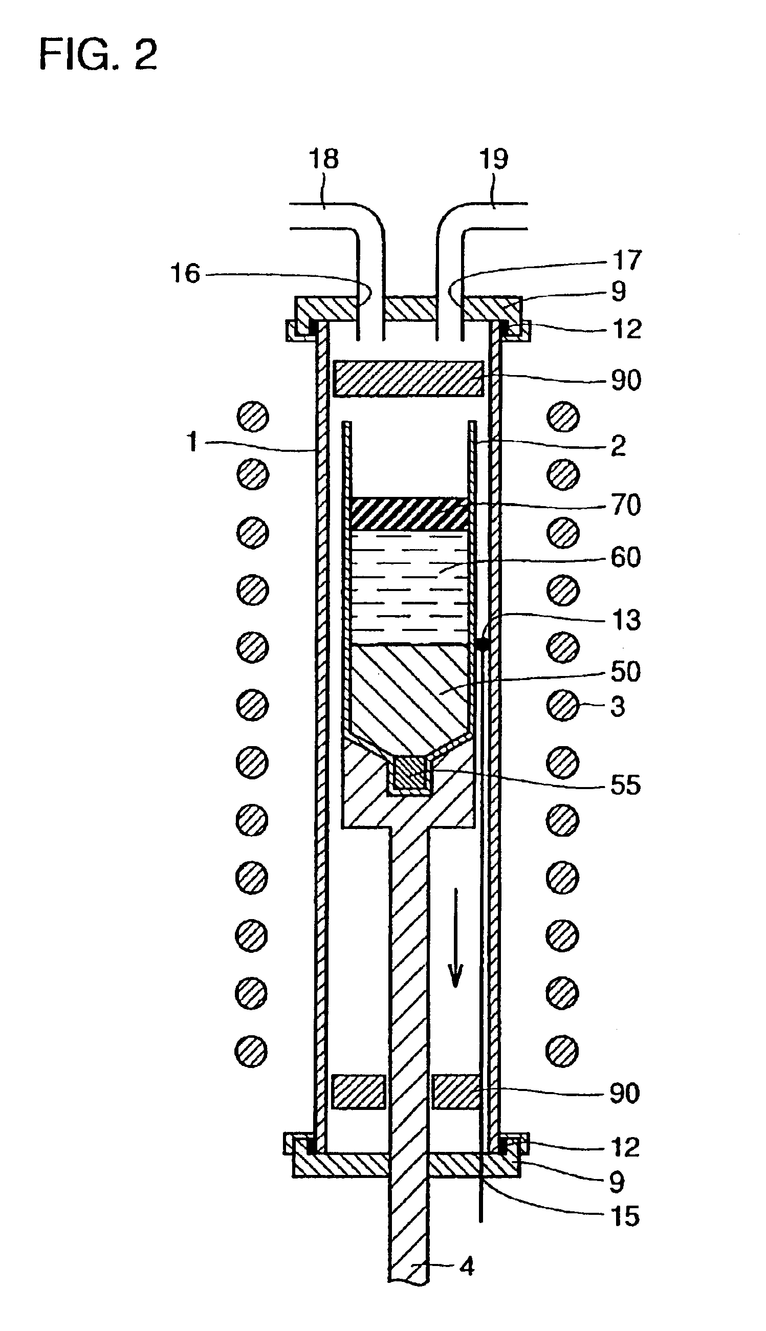
FIG. 8 is a sectional view showing a schematic structure of an apparatus of producing a semiconductor crystal according to a second embodiment of the present invention. The reactor tube of the second embodiment is formed of aluminum nitride.

Referring to FIG. 8, the apparatus has kanthal heater 3 of five zones divided into the upper one zone and the lower four zones by the interposition of a heat insulator 8. Heat insulator 8 is provided also inside aluminum nitride reactor tube 1 corresponding to the height of heat insulator 8 provided between the heater.

Crucible 2 is placed within aluminum nitride reactor tube 1 at the position lower than heat insulator 8. A reservoir 6 is placed in aluminum nitride reactor tube 1 at a position upper than heat insulator 8. A pipe 7 is connected to reservoir 6. Pipe 7 is formed so that the leading end is located in material melt 60 that is charged into crucible 2.

The remaining structure is similar to that of the apparatus of the first embodiment sho...

third embodiment

FIG. 12 is a sectional view showing a schematic structure of an apparatus of producing a semiconductor crystal according to a third embodiment of the present invention. The reactor tube of the present embodiment is formed of aluminum oxide.

The apparatus of FIG. 12 is mainly used in the pulling method. The apparatus includes an aluminum oxide reactor tube 1 having an open end at both end sides, and a heater 3 arranged around aluminum oxide reactor tube 1. A flange 9 is attached at both the open ends of aluminum oxide reactor tube 1.

Lower shaft 4 pierces the center of the flange 9 attached at the lower end of aluminum oxide reactor tube 1. Crucible 2 is mounted at the leading end of lower shaft 4. A pull shaft 14 that is movable upwards and downwards pierces the center of flange 9 attached at the upper portion of aluminum oxide reactor tube 1. A crystal is grown by drawing up pull shaft 4 in the direction of the arrow.

The apparatus of the present embodiment includes an aluminum oxide ...


PUM

PropertyMeasurementUnit
diameteraaaaaaaaaa
diameteraaaaaaaaaa
thicknessaaaaaaaaaa

Abstract

A large semiconductor crystal has a diameter of at least 6 inches and a low dislocation density of not more than 1×104 cm−2. The crystal is preferably a single crystal of GaAs, or one of CdTe, InAs, GaSb, Si or Ge, and may have a positive boron concentration of not more than 1×1016 cm−3 and a carbon concentration of 0.5×1015 cm−3 to 1.5×1015 cm−3 with a uniform concentration throughout the crystal. Such a crystal can form a very thin wafer with a low dislocation density. A special method and apparatus for producing such a crystal is also disclosed.

Description

BACKGROUND OF THE INVENTION1. Field of the InventionThe present invention relates to a semiconductor crystal, and a method and apparatus of producing the same. Particularly, the present invention relates to a semiconductor crystal for use in production of a GaAs substrate and the like employed in an optical device, an electronic device, and the like, and a method and apparatus of producing such a semiconductor crystal.2. Description of the Background ArtA GaAs crystal, for example, among the semiconductor crystals, is produced industrially by the pulling method (LEC (liquid Encapsulated Czochralski) method), the horizontal boat method (HB (Horizontal Bridgman) method, HGF (Horizontal Gradient Freeze) method), and the vertical boat method (VB (Vertical Bridgman) method, VGF (Vertical Gradient Freeze) method). The pulling method and the vertical boat method are particularly advantageous over the horizontal boat method for producing a single crystal since the yield is improved due to t...

Claims


Application Information

Patent Timeline
Patent Type & Authority Patents(United States)
IPC IPC(8): C30B11/00C30B15/00
CPCC30B11/00C30B15/00C30B29/42Y10T117/10Y10T117/1024Y10S117/90Y10T117/1096
Inventor KAWASE, TOMOHIROHASHIO, KATSUSHISAWADA, SHIN-ICHITATSUMI, MASAMI
Owner SUMITOMO ELECTRIC IND LTD
Why Eureka
Try Eureka