Method for producing quantum dot silicate thin film for light emitting device

a technology of light emitting devices and quantum dots, which is applied in the direction of electrolytic capacitors, nanoinformatics, semiconductor lasers, etc., can solve the problems of limiting the fabrication of group ii and vi compound semiconductors, unable to achieve the commercialization of devices fabricated by the above-mentioned techniques, and difficulty in controlling density and uniformity, so as to achieve high luminescence efficiency and increase the density of quantum dots

Active Publication Date: 2005-03-22
SAMSUNG ELECTRONICS CO LTD
View PDF8 Cites 52 Cited by
  • Summary
  • Abstract
  • Description
  • Claims
  • Application Information

AI Technical Summary

Benefits of technology

A feature of the present invention is to provide a quantum dot thin film having a high luminescence efficiency in which quantum dots are spaced apart from each other at a particular bonding distance and linked through siloxane covalent bonds formed therebetween to form a single film of the quantum dots, thereby increasing the density of the quantum dots in the thin film.
Another feature of the present invention is to provide a method for producing a quantum dot thin film which can maintain a bandgap of a single quantum dot without any clustering of quantum dots by mixing quantum dots and a silicate precursor having a functional group capable of interacting with the quantum dots.

Problems solved by technology

However, quantum dots synthesized by a vapor phase process based on lattice mismatch have an advantage in terms of good crystallinity, but have a disadvantage in that the control of density and uniformity is difficult.
Until now, it is known that devices fabricated by the above-mentioned techniques are unsuccessful in their commercialization.
However, compound semiconductor quantum dots synthesized by currently used wet chemistry techniques (colloidal process) are limited to the fabrication of Group II and VI compound semiconductors.
However, the reconfiguration of the quantum dots synthesized by the wet chemistry techniques is required to apply the quantum dots to most devices.
However, this simple mixing of the quantum dots and the organic polymer cannot increase the concentration of the quantum dots and improve the thermal stability of the quantum dots.
Accordingly, thin films produced from the quantum dots are limited in their applicability to various devices.

Method used


Image

  • Method for producing quantum dot silicate thin film for light emitting device
  • Method for producing quantum dot silicate thin film for light emitting device
  • Method for producing quantum dot silicate thin film for light emitting device

Examples


first embodiment

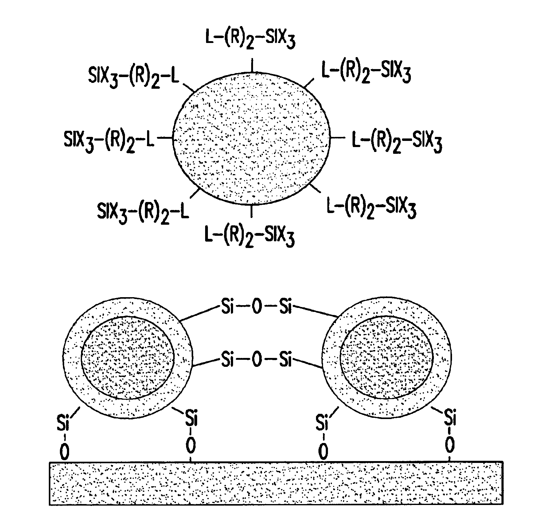
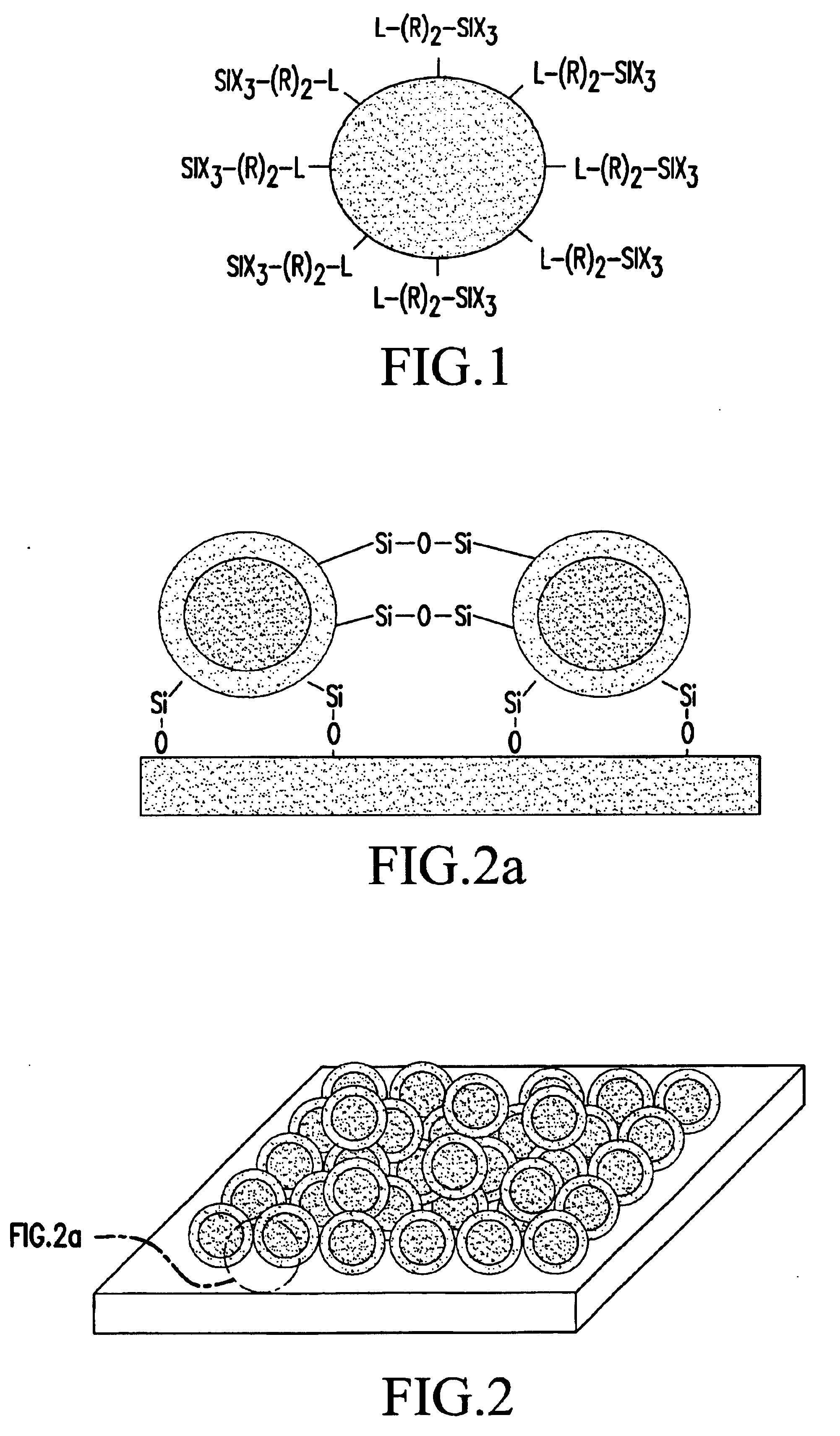
the present invention relates to a method for producing a quantum dot thin film with excellent mechanical and thermal stability by displacing the surface of nanometer-sized compound semiconductor quantum dots synthesized by a wet chemistry technique with a silane compound having at least one reactive group for a sol-gel process, and subjecting the surface-displaced quantum dots to a sol-gel process.

The method of the present invention will be explained in terms of the respective steps.

Synthesis of Quantum Dots

In the present invention, the synthesis of quantum dots can be performed by all techniques known in the art, and thus is not limited to the procedure as described below.

For the synthesis of nanometer-sized quantum dots in the state of a colloid by a wet chemistry technique, a solvent capable of stably dispersing quantum dots is used. The solvent used in the present invention must be able to be coordinated to the surface of quantum dots, and have a bulkiness to the extent that it...

second embodiment

the present invention relates to the method for producing a quantum dot silicate thin film by dispersing quantum dots synthesized by a wet chemistry technique in a silicate precursor compatible with the quantum dots, and coating the dispersion onto a substrate. The synthesis of the quantum dots is as explained above. The subsequent steps will be described below.

Preparation of Silicat Precursor

As a silicate precursor, a siloxane resin having a weight average molecular weight of about 1,000-100,000 and preferably about 1,000-10,000, is used. The silicate precursor is prepared by subjecting a silane compound having a phosphine-, amine- or thiol-based functional group and at least one reactive group for a sol-gel process, and a siloxane-based monomer to a sol-gel process under acidic or basic conditions. At this time, the sol-gel process involves hydrolysis and condensation. The molar ratio of the silane compound and the siloxane-based monomer is, preferably, 99:1-1:99.

As the siloxane-b...

example 1

Synthesis of Yellow Light-Emitting Cadmium Sulfide Quantum Dots

2.5 ml of trioctyl amine as a solvent is placed in a 25 ml flask equipped with a reflux condenser, and the temperature of the flask is adjusted to 180° C. with stirring. A solution of 50 mg of cadmium dithio diethyl carbamate in 0.9 ml of trioctyl phosphine is rapidly injected into the flask. After 10 minutes, a solution of 20 mg of zinc dithio diethyl carbamate in 0.3 ml of trioctyl phosphine is slowly added dropwise. About 5 minutes after the addition of zinc dithio diethyl carbamate is completed, the temperature of the reactor is cooled and then ethanol is added to quench the reaction. Quantum dots are obtained from the resulting mixture through centrifugation and dispersed in toluene. The photoluminescence spectrum confirmed that the compound semiconductor quantum dots emits yellow light at 536 nm.


PUM

PropertyMeasurementUnit
sizeaaaaaaaaaa
temperatureaaaaaaaaaa
sizeaaaaaaaaaa

Abstract

A method for producing a quantum dot silicate thin film for light emitting devices. The quantum dot silicate thin film is produced by introducing a silane compound having a functional group capable of interacting with a quantum dot and at least one reactive group for a sol-gel process into the surface of the quantum dot or a matrix material for dispersing the quantum dot, thereby exhibiting excellent mechanical and thermal stability.

Description

BACKGROUND OF THE INVENTIONThis non-provisional application claims priority under 35 U.S.C. § 119(a) on Korean Patent Application No. 2003-42448 filed on Jun. 27, 2003, which is herein incorporated by reference.FIELD OF THE INVENTIONThe present invention relates to a method for producing a quantum dot silicate thin film for light emitting devices, and more particularly to a method for producing a quantum dot silicate thin film for light emitting devices with excellent mechanical and thermal stability by introducing a silane compound having a functional group capable of interacting with a quantum dot and at least one reactive group for a sol-gel process, into the surface of the quantum dot or a matrix material for dispersing the quantum dot.DESCRIPTION OF THE RELATED ARTQuantum dots are nanometer-sized semiconducting materials which exhibit quantum confinement effects. When the quantum dots are irradiated by light from an excitation source to reach respective energy excited states, t...

Claims


Application Information

Patent Timeline
Patent Type & Authority Patents(United States)
IPC IPC(8): B82B3/00C09K11/00C09K11/88C09K11/89C09K11/08C09K11/56G01N33/53H01L21/368H01L21/00H01L21/20H01L21/02H01L29/02H01L29/06H01L33/00H01S5/00C08G77/22C08G77/00H01L33/06H01L33/28H01L33/44
CPCB82Y5/00B82Y10/00B82Y30/00C09K11/565B82Y20/00Y10S438/962H01L21/20
Inventor YIM, JIN HEONGJANG, EUN JOOAHN, TAE KYUNG
Owner SAMSUNG ELECTRONICS CO LTD
Why Eureka
Try Eureka